Months into the project and I was still amazed at the lack of availability of a class of ASICs: USB-I2S bridges. Well I just lied — if you are fine with USB 1.1 (12 Mbit/s, the so-called “Full Speed”) and USB Audio Class (UAC) 1.0, which severely limits your (bit depth × resolution × channel count), then there are countless chips out there, both ASIC and general-purpose microcontrollers, at various level of integration. You might not be able to source prototype quantities from Digikey/Mouser (e.g. the CM103 chip on the cheap dongle I bought on Aliexpress, or various offerings from Sabre/ESS/Via), but they’re there. Some even support 24 bit 96 kHz. A lot of them derive their audio clocks from built-in XO and PLL, sometimes shared with USB, which leads to poor quality…
So what do I care about then?
Spec
- USB Audio Class (UAC) 2.0
- ≥ 2 output channels
- 24 bit 192 kHz support
- external master clock option
Well, I betrayed myself by asking for 192 kHz, as in the very first post I explicitly said 96 kHz is way good enough. The reasoning: My DAC chip already supports 192 kHz, and I don’t want the digital source to be the bottleneck. So even if I end up using 96 kHz for best analog performance, I want the system to be capable of operating at the max data rate supported by the DAC.
MCU Picks
UAC 2.0 means USB 2.0 High Speed (480 Mbit/s). There are only a few budget and/or low-footprint choices:
- Atmel SAM3U: Other than USB, this is just yet another Cortex-M3 chip (which is a good thing!). However it comes in bulky 100-/144-pin QFP/BGA packages.
-
Cypress FX2LP (CY7C68013/4/5/6): 8-bit 8051-derivative core (similar to Dallas Semiconductor DS80C320) running at 48 MHz. Turtle slow, few peripherals, but it comes in a tiny 56-pin QFN package (although it does require an external I2C EEPROM, available in TSSOP8).
-
XMOS XS1-U8 series: Hugely popular in the “audiophile” market. It is one of these “many small cores” niche market MCUs. Didn’t do much homework though — will explain later.
While I am very comfortable with Cortex-M3 due to past experience, its footprint is way too huge for the project at hand, so I went for CY7C68013. In fact I had known this chip for quite a long time, as it frequently appears in the BOM of budget FPGA-based designs that provides USB connectivity. Heck — even Saleae Logic is (yet another) Spartan 6 + CY7C68013! There doesn’t seem to be a good standalone minimal system board for it though, so I quickly made one:

I intended to attach a small CPLD for I2S output, but still there is a lot of work, especially when I have to write 8051 (!) firmware for CY7C68013 (yes, more annoying than Verilog for CPLD!) that sets up the whole UAC 2.0 streaming…
How About Easier, Sensei?
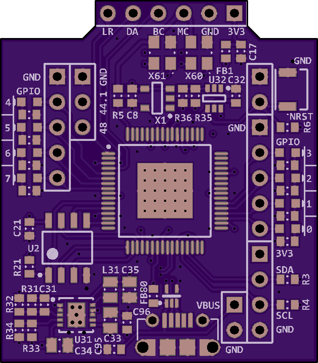
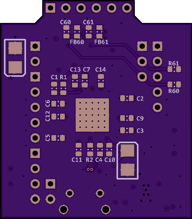
Well, the focus of this DAC project is, of course, the DAC itself and the associated analog circuits. USB-I2S is more like a necessity — an inevitable chore I have to bolt on to make the system complete. So I kept looking for ASICs, and I found one that is close enough: XMOS XHRA-2HPA. It even comes with a reference design that does exactly what I want (albeit with a crappy all-integrated DAC)! This chip is clearly based on a normal XMOS XS1-U8 with a custom bootloader, but the similarity ends here — it loads encrypted (!) firmware from external Quad SPI flash, and is therefore completely locked down (not user-programmable), so by duck typing it is an ASIC. On the other hand, I don’t have to program it. Sounds like a fair deal. While the reference design was fully integrated, I instead isolated the XHRA minimal system and made a PCB.
XHRA Hiccups — the SPI Flash Fiasco
What was supposed to be a turn-key solution turned into a prolonged attrition debugging warfare lasting well beyond 2 PCB turnarounds, just to make this thing $profanity-ing boot and enumerate! And each time, the culprit turned out to be that innocent-looking, friendly-packaged, 8-pin SOIC Quad SPI Flash.
Quick TL;DR:
- There is a whitelist for SPI Flash ID bytes.
- The “correct” SPI flash does not have built-in
HOLD# pull-up resistor.
- SPI clock runs at 2.4 MHz at first, but eventually switches to 100/6 = 16.667 MHz .
- The “nibble ordering” mention in the datasheet is misleading.
$profanity Bus Pirate.
Apparently, being “pin and instruction compatible” is not good enough — there is a whitelist for IDs. If the wrong ID is returned, the chip drops dead. There is one vague mention of this on the datasheet, and I only realized its true meaning after I dug into a logic analyzer capture run and actually inspected the SPI transfers. Turned out that right before the chip fell silent, it had repeatedly sent command 0x9F over SPI — “read chip ID”. D’oh!
The reason I didn’t look at the logic analyzer output? 16 MHz is too fast for my old good Saleae Logic 16 streaming 6 channels at its max 50 MHz sample rate (because Nyquist). Miscaptures were frequent, but I was lucky that run.
Then there is another misleading information from the datasheet stating that the SPI flash needs to store the least significant nibble (4 bits) of a byte (8 bits) first, which sounds as if before programming we need to manually swap the nibbles for all the bytes… Turns out you don’t have to do anything other than following the datasheet, which clearly transfers MSnibble before the LSnibble on the 4-bit SPI bus. D’oh!
I once wrote a blog post on SPI flash programming using Bus Pirate — and of course I was trying to program this. Eventually I figured out that Bus Pirate is too unreliable (on top of slow) for flash programming, so I bought a dirt cheap dedicated flash programmer on Aliexpress (again), which of course is based on STM32F1, as most things coming from China do these days[citation needed]. Never felt so good about being a native Chinese speaker when I clicked through that Windows 98-inspired GUI in GBK-encoded Simplified Chinese, like a boss™.
Note that blank SPI flash chips usually come with 4-bit (quad) SPI disabled, and requires a manual write to a status register to enable it. Since this flash programmer does not do this for me, till this day I still perform this ceremony using my Bus Pirate.
BONUS: The configuration bytes / firmware image generator of XHRA, downloadable from the reference design page, takes as input a config file with .cfg extension. Public service time: It is a Python script. Have fun.
End of Rant
And here’s the minimal system board on OSHPark, and here is the raw BOM full of placeholders. {X60 = 24.576 MHz, X61 = 22.5792 MHz} can be any pin 1 active high enable, 3.2 × 2.5 mm SMD XO.