Cubic GaN offers to break away from traditional approaches and meet (if not exceed) the future semiconductor device efficiency trends on scalable silicon platforms.
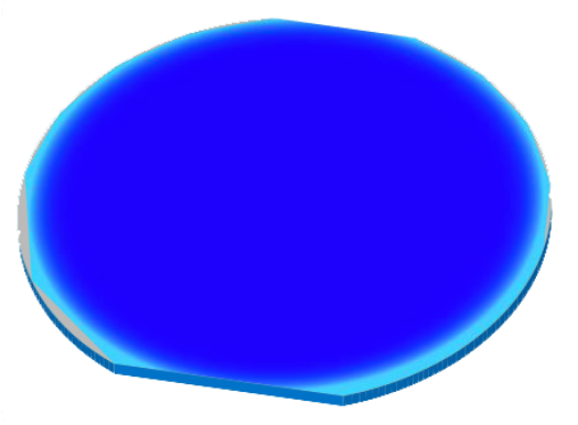
Freestanding
Cubic GaN
Engineered substrates for RF, Power Electronics, and Photonics
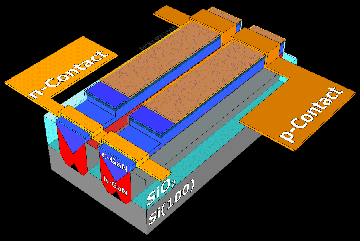
Light Emitting
Diodes
For solid-state lighting and visible emitters
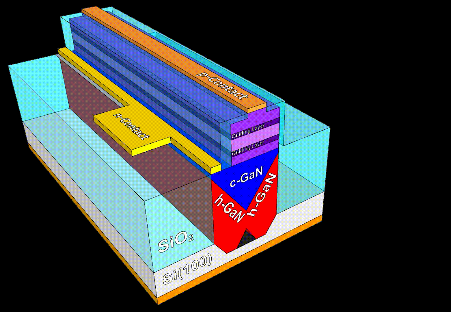
Laser Diodes
For displays and communication
Technology
Proprietary silicon patterning compatible with industrious platforms.
Advantages
Company
Technology
Scaling
Proprietary technology on Si (100)
Compatible with Si scaling (i.e. 12-inch)
Others
On conventional substrates (i.e. sapphire, SiC, Si (111))
Restricted to specialized fabs (typically, 8-inch)