Inspiration
We've all waited weeks for a PCB to arrive, only to find it doesn't work due to a simple schematic error—a floating power label, missing capacitor or wrong pin connection. These mistakes cost hundreds of dollars and weeks of delay per re-spin. Software has linting tools like ESLint that catch errors before runtime. Hardware doesn't. KiCad's DRC only catches electrical violations, not functional errors and we wanted to create a tool that truly understands circuits and can say "your timer won't oscillate because R1 isn't connected correctly"—not just "net has an error."
What it does
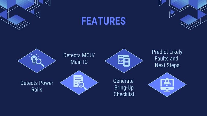
PreFab analyzes KiCad schematics before fabrication to catch design errors:
Workflow: Upload .kicad_sch file → AI analyzes circuit → Get risk score + fixes
Analysis:
- AI identifies circuit type (STM32 board, etc.)
- Runs 20+ checks (covers the main functional aspects of a PCB bring-up): power connectivity, signal integrity, timing, MCU configuration
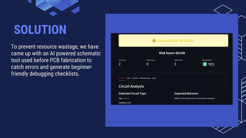
- Calculates risk score (0-100) and severity levels
- Determines if board is safe to power on
Output: Specific issues with component references and fix instructions Interactive bring-up checklist Expected behavior (frequencies, voltages, duty cycles) Exportable JSON/Markdown reports
Example: Upload a schematic of a timer with disconnected power → Detects astable multivibrator, flags critical power issue, calculates 5.5Hz output, provides step-by-step fix checklist.
How we built it
Tech Stack: Python, Streamlit, OpenAI API, Google Gemini
Key Components:
- Custom KiCad Parser: S-expression parser to extract components, wires, and connections
- Netlist Builder: Traces electrical connections with spatial tolerance matching
- 20+ Analysis Functions: Modular checks for power, signal, timing, and MCU issues
- AI Integration: OpenAI → Gemini → Heuristics fallback chain with structured JSON output
- Web Interface: Streamlit UI with progress tracking, interactive dashboard, and export
Challenges we ran into
KiCad Parsing: S-expression format poorly documented. Had to reverse-engineer from example files and handle edge cases like multi-unit components. Netlist Algorithm: Matching wire segments with spatial tolerance while handling junctions, crossings, and labels was complex. Solved with spatial indexing. AI Reliability: Early prompts gave inconsistent JSON. Fixed with strict schemas, examples, validation, and heuristic fallback. Analysis Accuracy: Functions needed to work across circuit styles (different power pin names, multiple voltage rails). Used flexible pattern matching. Performance: LLM calls take 5-15 seconds. Added progress bars, caching, and instant heuristic mode.
Accomplishments that we're proud of
Robust AI integration with automatic fallback (OpenAI → Gemini → Heuristics) and graceful degradation Modular architecture that add new analysis functions without touching core code where the LLM auto-discovers them
What we learned
Technical: S-expression parsing, spatial algorithms for netlist building, LLM prompt engineering for structured output, Streamlit session state management Hardware: Common PCB mistakes, gap between "electrically correct" (DRC) and "functionally correct" (works), patterns in debugging workflows AI/ML: LLMs understand circuit topology well with context, structured output + validation essential, fallback strategies critical, hybrid AI + deterministic analysis works best Product: Color coding improves scanning, progress bars crucial for >3 sec operations, export functionality, modular architecture enables parallel development
What's next for PCB Debugger
- PCB layout analysis (trace widths, via placement)
- Enhanced functions: thermal analysis, EMI checks, signal integrity
- KiCad plugin for in-editor validation


Log in or sign up for Devpost to join the conversation.