Six Ground Symbols and What Each One Promises

Full article on JLCPCB: https://jlcpcb.com/blog/ground-symbols-explained

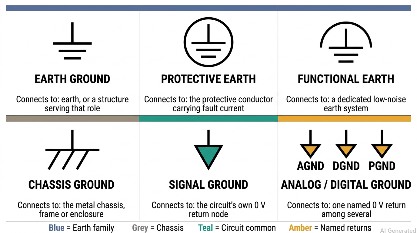
Four ground marks are numbered in IEC 60417: 5017 earth, 5018 functional earth, 5019 protective earth, 5020 chassis. Only 5019, the earth mark inside a circle, may identify a protective earth terminal. Use 5018 there instead and you have not made a drafting slip, you have made a compliance failure.

8779427690647126016

Quick-reference chart of all six ground symbols with their standard numbers

The Six Marks

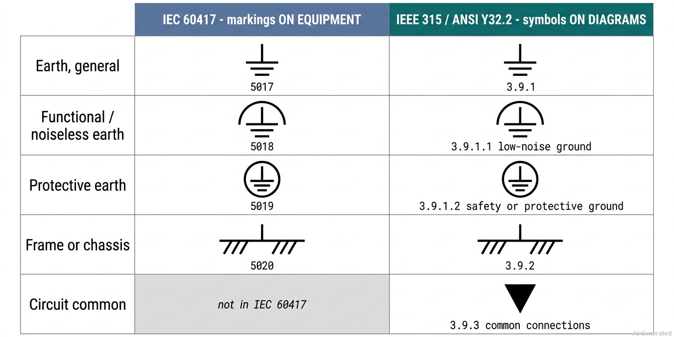
Six symbols cover almost every schematic and equipment label. Four are numbered by IEC 60417, which standardises markings placed on equipment; the other two come from IEEE 315, which standardises symbols drawn on diagrams.

· 5017, three shrinking bars — earth, general (IEEE 315 clause 3.9.1)

· 5018, earth mark under an arc — functional or noiseless earth (3.9.1.1)

· 5019, earth mark inside a circle — protective earth (3.9.1.2)

· 5020, bar with three angled strokes — chassis or frame (3.9.2)

· Triangle, solid or hollow — signal or common ground (clause 3.9.3)

· Triangle lettered AGND, DGND or PGND — one named 0 V return among several

8779427643767390208

IEC 60417 and IEEE 315 ground symbols compared side by side

Where the Stem Stops

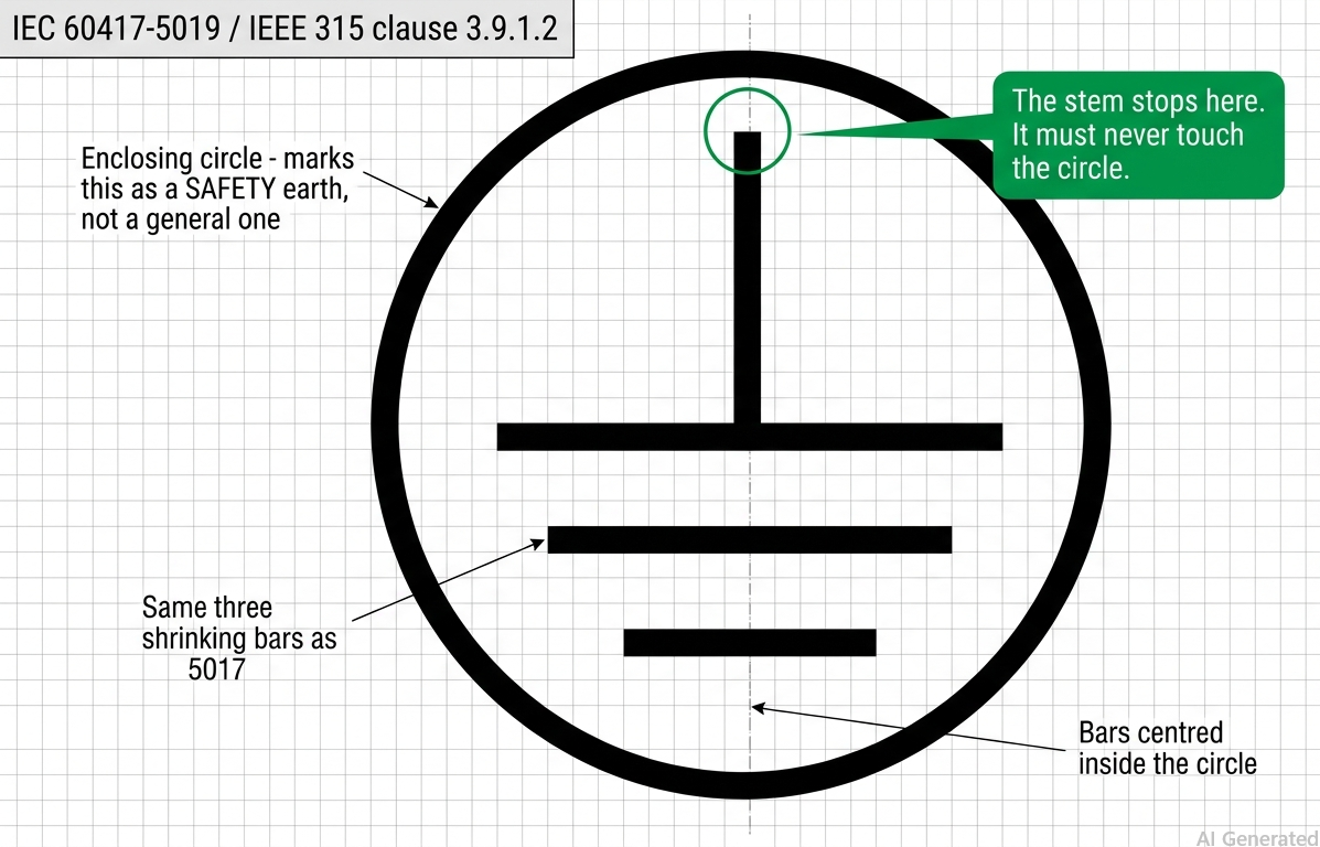
One drawing detail separates a correct protective earth mark from the most widely copied error in the industry. In IEC 60417-5019 the vertical stem stops inside the circle and never touches it. The 2011 edition of NFPA 70, the US National Electrical Code, carried an informational note figure for an equipment grounding conductor termination point drawn with the bar touching the circle. Two further tells: the 5017 bars must shorten as they descend, and 5018 never substitutes for 5019.

8779427738011234304Image

The protective earth symbol, stem stopping short of the circle

Net Names Win

In every mainstream EDA tool the net name decides what connects, not the picture. Altium states it plainly: the net name determines which net a power port joins, not the style of the symbol. Three ports drawn as Earth, Bar and Signal Ground all land on GND if all three are named GND. To create a genuinely separate return, name it AGND everywhere it belongs, join it to GND at exactly one point with a 0 Ω link or net tie, then run ERC and confirm two nets joined once.

The full six-symbol chart, the IEC 60417 versus IEEE 315 mapping and the tool-by-tool net rules for KiCad, Altium and EasyEDA are in the complete guide: Read the full guide

Makers & Education Spaces
Resistor Types and the Spec Most BOMs Skip

Full article on JLCPCB: https://jlcpcb.com/blog/complete-guide-to-resistor-types

Tolerance is a day-one, room-temperature number. TCR is what you actually live with. A ±1% resistor at 200 ppm/°C can move another ±1% across a 50 °C rise, so its real in-circuit accuracy is worse than its label — and TCR is the column most engineers never filter on.

8779427257617031168

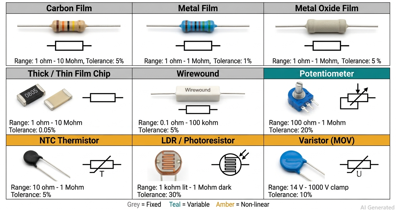
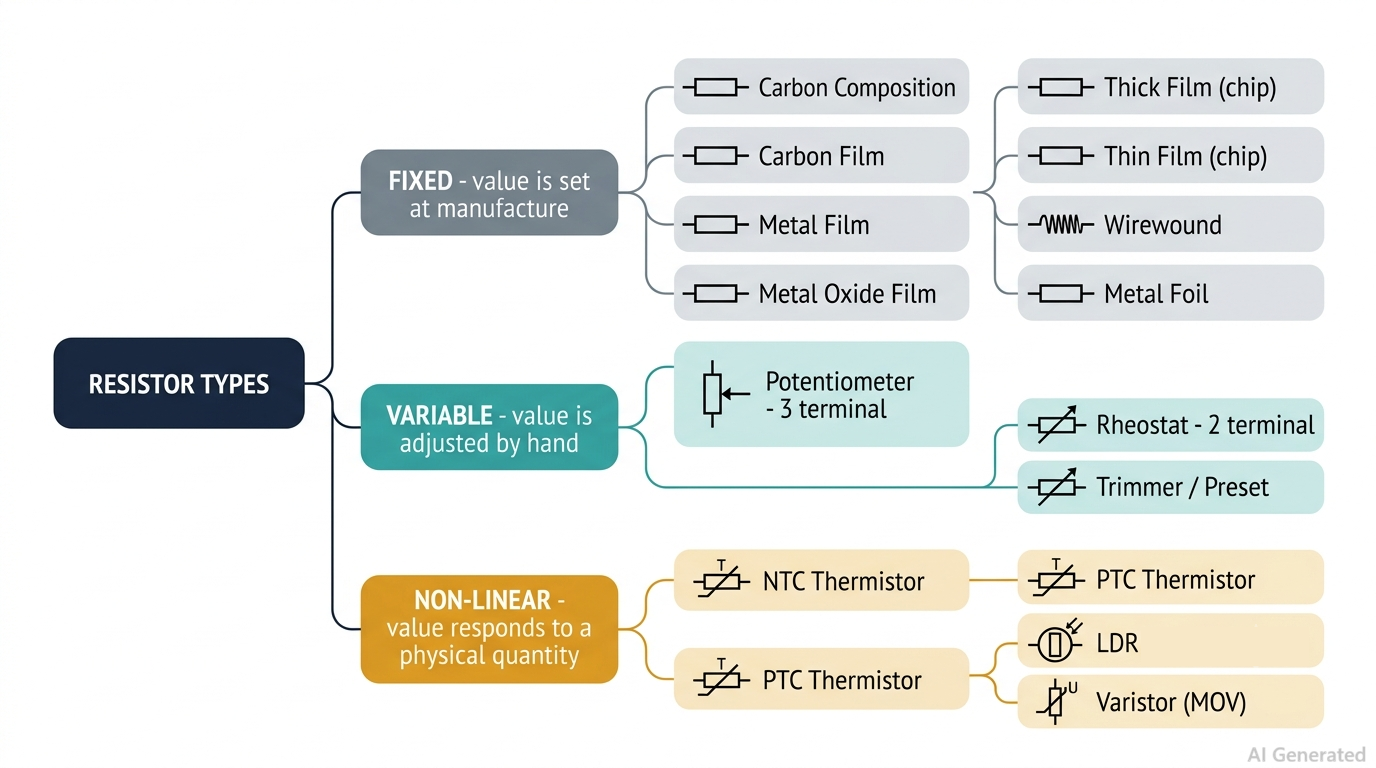
Resistor types chart — fixed, variable and non-linear families with their symbols

Three Families

Every resistor sorts into one of three branches. Fixed types hold a value, judged on tolerance, TCR and power. Variable types expose a wiper, judged on track material and rotational life. Non-linear types are transducers — read the curve, not a tolerance figure.

· Carbon film: ±2% to ±5%, TCR −200 to −1000 ppm/°C

· Metal film: ±0.1% to ±1%, TCR ±25 to ±100 ppm/°C

· Thick film chip: ±1% to ±5%, TCR ±100 to ±200 ppm/°C

· Thin film chip: ±0.05% to ±0.5%, TCR ±5 to ±25 ppm/°C

· Wirewound: ±0.005% to ±5%, 1 W to 300 W and beyond

· Metal foil: ±0.001% to ±0.01%, TCR 0.2 to 2 ppm/°C

8779427229947072512

Classification tree from fixed, variable and non-linear down to each resistor type

The 200-Cycle Trap

Track material sets the quality, but the specification nobody prints is rotational life. A panel potentiometer is rated for 10,000 to 1,000,000 cycles. A trimmer is often rated for 200. Put a trimmer behind a user-accessible knob and the track wears through inside a year, and a worn track produces a scratchy, intermittent, open-circuit wiper that gets blamed on everything except the pot. Trimmers are set-once parts; a 25-turn cermet trimmer exists to null an offset and then be left alone.

Choosing Fast

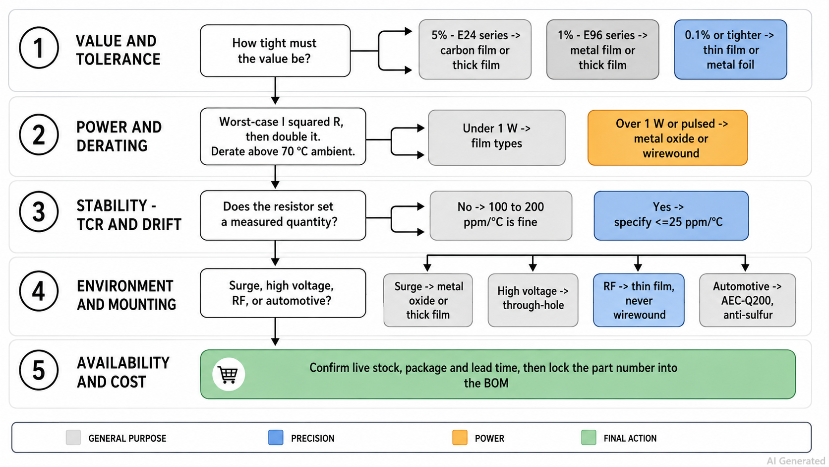
Work five filters in order and you finish choosing between two parts, not twenty. Fix value and tolerance first, rounding to a stocked E-series value under IEC 60063 — E24 for ±5%, E96 for ±1% and tighter. Size power at worst-case I²R and pick a part rated for at least twice it, because ratings are quoted at 70 °C ambient and fall from there. Filter on TCR before tolerance whenever the resistor sets a measured quantity. Surge-exposed inputs get metal oxide or thick film, never thin film.

8779427192657547264

The five-step resistor type selection flowchart

The full resistor types chart, all seven fixed families and the application-by-application selection table are in the complete guide: Read the full guide

Electronic Tips & Projects
Power Supply Symbols, Circles and Diamonds

Full article on JLCPCB: https://jlcpcb.com/blog/power-supply-symbols-ultimate-guide

A circle, a diamond, and three shrinking horizontal bars. Three power supply symbols, three different meanings, and only one of them is an independent source. Draw a controlled source as a circle and your simulation settles on a completely wrong operating point. Neither that error nor an implicit chassis-to-earth tie trips a design rule check.
8779426723897937920

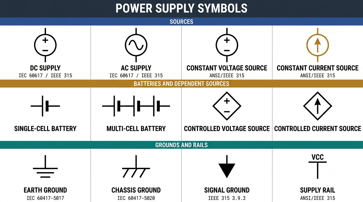
The power supply symbol chart: DC, AC, source, battery and ground symbols side by side

Four Symbol Families

Fourteen symbols cover almost every power source you will meet on a schematic, and they sort into four families: sources, batteries, grounds and rail labels. The outline answers the first question before you read a single label.

· Circle: independent source. Polarity marks for DC, a sine wave for AC, an arrow for current

· Diamond: dependent source, output set by another circuit quantity

· Unequal bar pairs: battery. The long thin bar is positive, one pair per cell

· Earth ground: three shrinking bars, IEC 60417-5017, IEEE 315 clause 3.9.1

· Chassis ground: one bar with three angled strokes, IEC 60417-5020, clause 3.9.2

· Signal ground: downward triangle, IEEE 315 clause 3.9.3
8779426655040049152

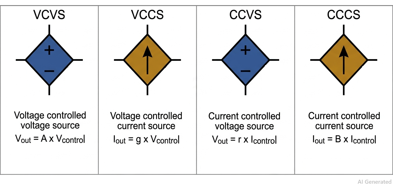
The four dependent source symbols drawn as diamonds with their controlling variables

Why A Diamond

The diamond outline is the only visual difference between a controlled source and an independent one. VCVS and CCVS carry polarity marks; VCCS and CCCS carry an arrow. This is how every active device is modelled: a bipolar transistor is a CCCS, a MOSFET is a VCCS, an ideal op-amp is a VCVS, and a current-sense amplifier behaves as a CCVS. One caveat. The diamond is a drafting convention, not a numbered entry in IEC 60617 the way the earth mark is numbered in IEC 60417, so treat it as binding practice but never cite a clause number for it.
8779426572682723328

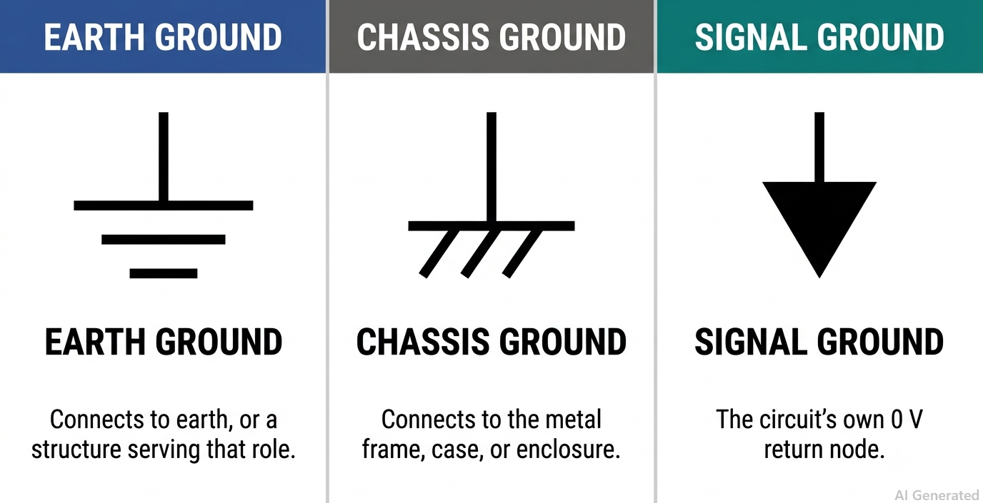
Earth, chassis and signal ground symbols drawn at equal scale for comparison

Three Grounds

Earth, chassis and signal ground are three separate nets. IEEE 315 clause 3.9.2 notes explicitly that a chassis may sit at a substantial potential relative to the earth around it, so placing both glyphs on one net without an explicit bond creates a ground loop that shows up as a failed EMC scan rather than a DRC error. AGND, DGND and PGND all reuse the signal ground triangle, and only the label changes. That is what lets a layout tool keep three returns apart and join them at one defined tie point. If you cannot find that tie point, the schematic has a defect.

The full 14-symbol chart, the IEC 60617 versus ANSI/IEEE 315 comparison, the four dependent source equations and the symbol-to-footprint table are in the complete guide: Read the full guide

Equipment & Tools & Resources
Logic Gate Symbols, ANSI vs IEC

Full article on JLCPCB: https://jlcpcb.com/blog/logic-gate-symbols-guide

The same NAND gate appears as a bubbled D-shape in one schematic and a rectangle marked & in the next. Neither is wrong. ANSI/IEEE Std 91-1984 defines both families, so calling the rectangle the non-ANSI form is a review comment worth dropping. What actually flips your output is the bubble.

8779426056187740160

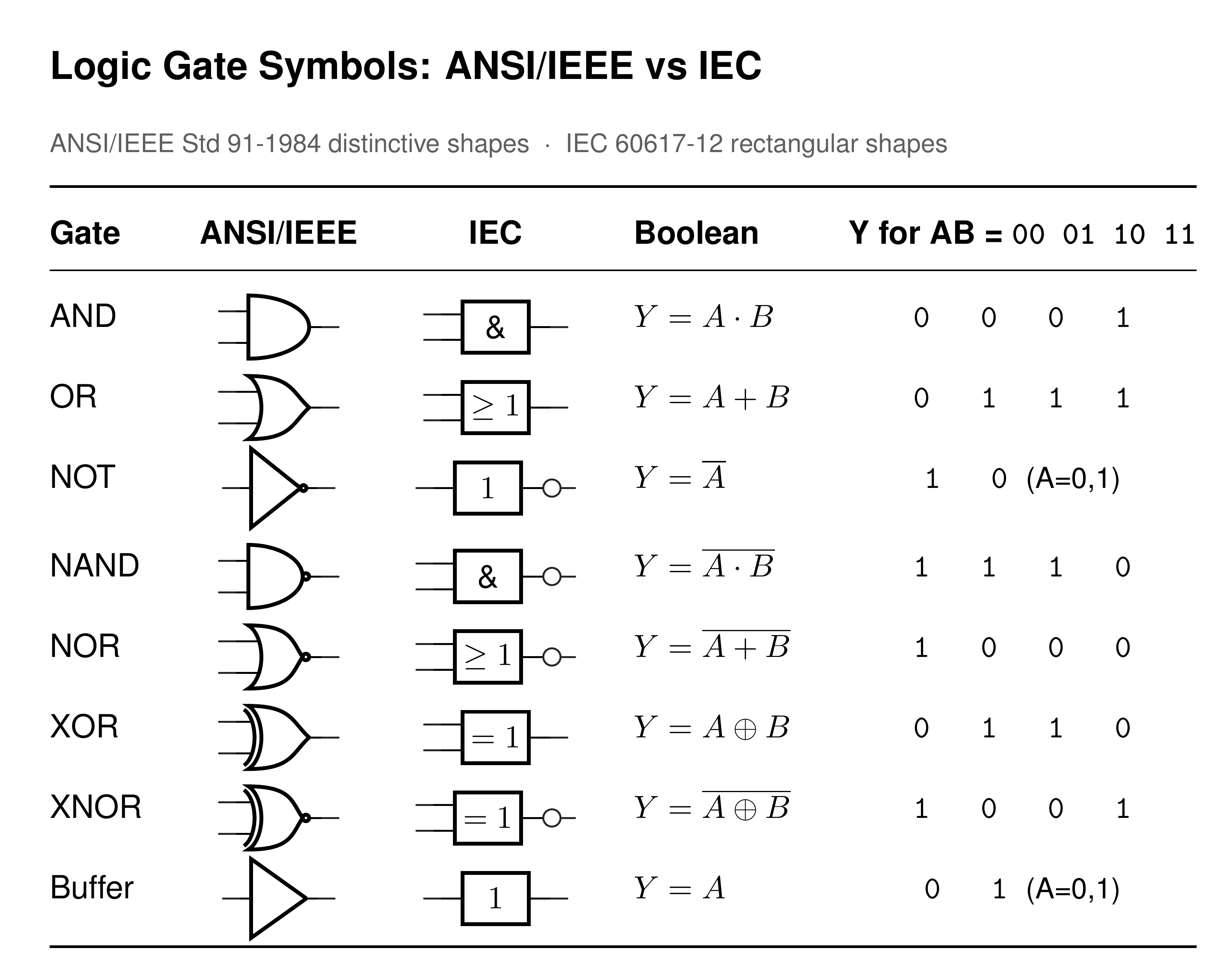
Every logic gate in ANSI distinctive shape and IEC rectangular form, side by side

Two Symbol Sets

The distinctive shapes came from MIL-STD-806 in the early 1960s and passed into ANSI/IEEE Std 91-1984. IEC 60617-12 standardised the rectangle, which names the function with a qualifying symbol printed inside it rather than by outline. Pick one set per drawing set, and never mix both on a sheet: a reviewer scanning for shapes will skip a rectangle.

· AND: flat back, curved nose. IEC qualifier &

· OR: curved back, pointed nose. IEC qualifier at least 1

· XOR: OR shape, doubled input line. IEC qualifier =1

· NOT and buffer: triangle, with and without the bubble. IEC qualifier 1

· NAND, NOR, XNOR: the same outlines with an output bubble

· Rail range decides the family: 74HC runs 2 V to 6 V, 4000B runs 3 V to 18 V

8779426096398397440

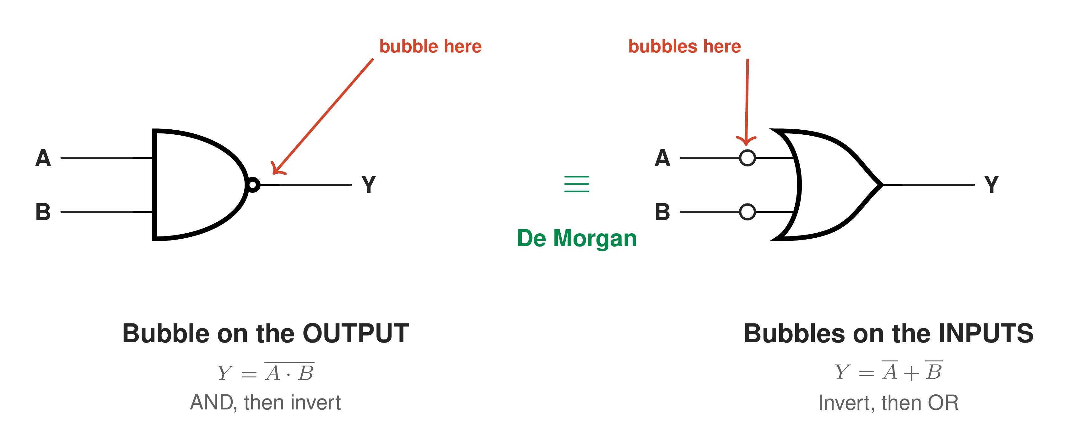
Inversion bubble anatomy, output bubble compared with input bubbles on the same gate

Reading The Bubble

The small circle is a negation indicator, not decoration. On an output it complements the function, so AND becomes NAND and OR becomes NOR. On an input it marks that pin active LOW, and the gate sees the inverted net. An OR shape with bubbles on both inputs is the same gate as a NAND, because (A · B)' = A' + B'. That De Morgan equivalent is drawn deliberately, so the bubbles line up with active-low net names such as nCS or /OE. A wedge instead of a circle marks an active-low pin without inverting the function.

8779426012124549120

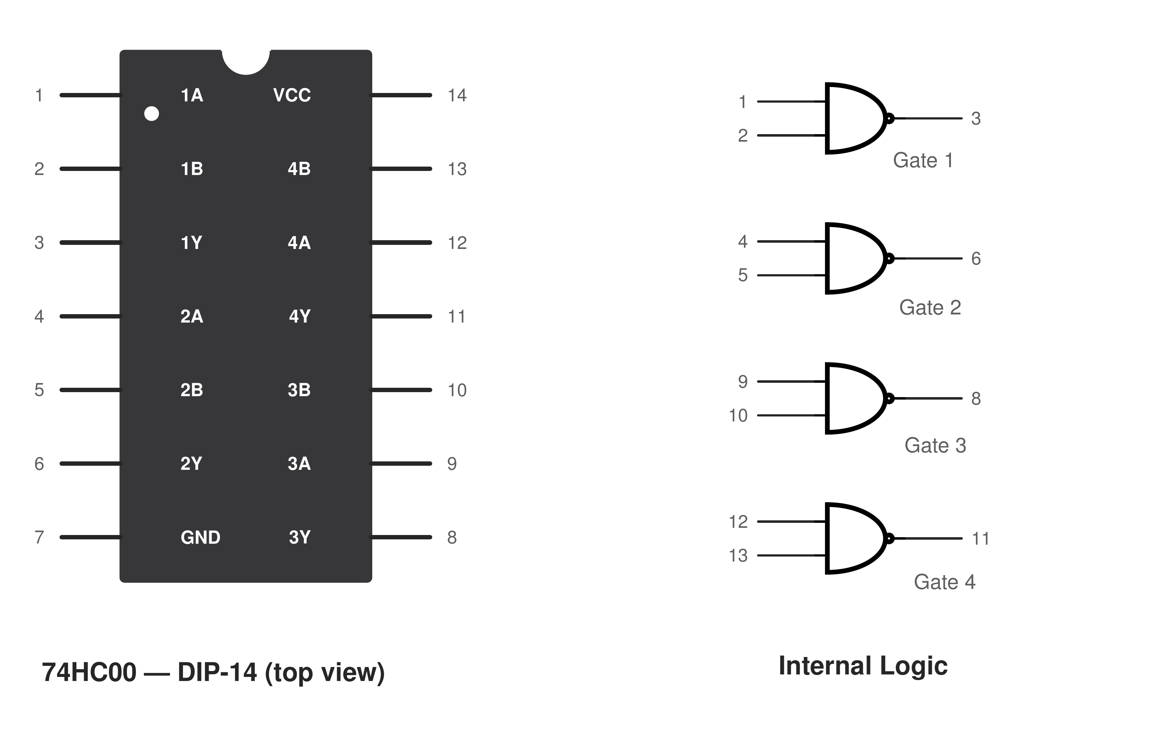
74HC00 quad 2-input NAND pinout, 14-pin package

Symbol To Package

One symbol is rarely one part. A 74HC00 quad NAND is U1A to U1D on the schematic and a single SOIC-14 on the layout, sharing one VCC pin and one decoupling capacitor. Tie every unused CMOS input to VCC or GND, because a floating input self-biases, oscillates and raises supply current. Do not assume pin compatibility either: the 74HC02 places its outputs on pins 1, 4, 10 and 13, so it cannot share a 74HC00 footprint.

The full ANSI and IEC chart, all eight truth tables, the NAND-only gate counts and the 74xx to 4000-series part lookup are in the complete guide: Read the full guide

FPGA & Programmable Logic