Image

Bare Metal STM32: Increasing The System Clock And Running Dhrystone

When you start an STM32 MCU with its default configuration, its CPU will tick along at a leisurely number of cycles on the order of 8 to 16 MHz, using the high-speed internal (HSI) clock source as a safe default to bootstrap from. After this phase, we are free to go wild with the system clock, as well as the various clock sources that are available beyond the HSI.

Increasing the system clock doesn’t just affect the CPU either, but also affects the MCU’s internal buses via its prescalers and with it the peripherals like timers on that bus. Hence it’s essential to understand the clock fabric of the target MCU. This article will focus on the general case of increasing the system clock on an STM32F103 MCU from the default to the maximum rated clock speed using the relevant registers, taking into account aspects like Flash wait states and the APB and AHB prescalers.

Although the Dhrystone benchmark is rather old-fashioned now, it’ll be used to demonstrate the difference that a faster CPU makes, as well as how complex accurately benchmarking is. Plus it’s just interesting to get an idea of how a lowly Cortex-M3 based MCU compares to a once top-of-the line Intel Pentium 90 CPU.

Continue reading “Bare Metal STM32: Increasing The System Clock And Running Dhrystone”

A circuit diagram in a book on a desk with computers and microcontrollers

Taking Electronics To A Different Level

One part wants 3.3V logic. Another wants 5V. What do you do? Over on the [Playduino] YouTube channel, there’s a recent video running us through a not-so-recent concern: various approaches to level-shifting.

In the video, the specific voltage domains of 3.3 volts and 5 volts are given, but you can apply the same principles to other voltage domains, such as 1.8 volts, 2.5 volts, or nearly any two levels. Various approaches are discussed depending on whether you are interfacing 5 V to 3.3 V or 3.3 V to 5 V.

Continue reading “Taking Electronics To A Different Level”

Image

TinyCore Board Teaches Core Microcontroller Concepts

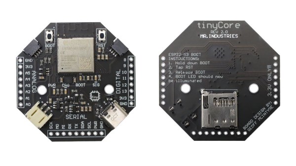
Looking for an educational microcontroller board to get you or a loved one into electronics? Consider the tinyCore – a small and nifty octagon-shaped ESP32 board by [MR. INDUSTRIES], simplified for learning yet featureful enough to offer plenty of growth, and fully open.

The tinyCore board’s octagonal shape makes it more flexible for building wearables than the vaguely rectangular boards we’re used to, and it’s got a good few onboard gadgets. Apart from already expected WiFi, BLE, and GPIOs, you get battery management, a 6DoF IMU (LSM6DSOX) in the center of the board, a micro SD card slot for all your data needs, and two QWIIC connectors. As such, you could easily turn it into, say, a smartwatch, a motion-sensitive tracker, or a controller for a small robot – there’s even a few sample projects for you to try.

You can buy one, or assemble a few yourself thanks to the open-source-ness – and, to us, the biggest factor is the [MR.INDUSTRIES] community, with documentation, examples, and people learning with this board and sharing what they make. Want a device with a big display that similarly wields a library of examples and a community? Perhaps check out the Cheap Yellow Display hacks!

Continue reading “TinyCore Board Teaches Core Microcontroller Concepts”

Image

Super Simple Deadbuggable Bluetooth Chip

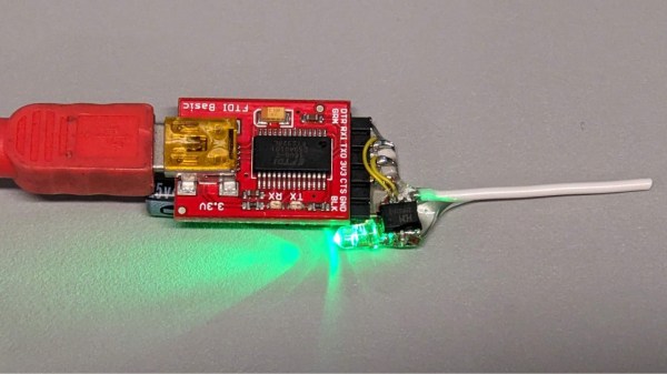
We’re all used to Bluetooth chips coming in QFN and BGA formats, at a minimum of 30-40 pins, sometimes even a hundred. What about ten pins, with 1.27 mm pitch? [deqing] from Hackaday.io shows us a chip from WCH, CH571K, in what’s essentially a SO-10 package (ESSOP10). This chip has a RISC-V core, requires only three components to run, and can work Bluetooth through a simple wire antenna.

This chip is a RISC-V MCU with a Bluetooth peripheral built in, and comes from the CH57x family of WCH chips that resemble the nRF series we’re all used to. You get a fair few peripherals: UART, SPI, and ADC, and of course, Bluetooth 4 with Low Energy support to communicate with a smart device of your choice. For extra hacker cred, [deqing] deadbugs it, gluing all components and a 2.54 mm header for FTDI comms onto the chip, and shows us a demo using webBluetooth to toggle an LED through a button in the browser.

You need not be afraid of SDKs with this one. There’s Arduino IDE support (currently done through a fork of arduino_core_ch32) and a fair few external tools, including at least two programming tools, one official and one third-party. The chip is under a dollar on LCSC, even less if you buy multiple, so it’s worth throwing a few into your shopping cart. What could you do with it once received? Well, you could retrofit your smoke alarms with Bluetooth, create your own tire pressure monitors, or just build a smartphone-connected business card!

A dynamic light box for F1 events, built like the F1 logo.

F1 Light Box Helps You Know The Current Race Status

[joppedc] wrote in to let us know that the Formula 1® season is coming to an end, and that the final race should be bangin’. To get ready, he built this ultra-sleek logo light box last week that does more than just sit there looking good, although it does that pretty well. This light box reacts to live race events, flashing yellow for safety cars, red for red flags, and green for, well, green flags.

Continue reading “F1 Light Box Helps You Know The Current Race Status”

Image

Standalone USB-PD Stack For All Your Sink Needs

USB PD is a fun protocol to explore, but it can be a bit complex to fully implement. It makes sense we’re seeing new stacks pop up all the time, and today’s stack is a cool one as far as code reusability goes. [Vitaly] over on Hackaday.io brings us pdsink – a C++ based PD stack with no platform dependencies, and fully-featured sink capabilities.

Continue reading “Standalone USB-PD Stack For All Your Sink Needs”

[Piers] explains his code

A Deep Dive Into Using PIO And DMA On The RP2350

Here’s a fun rabbit hole to run down if you don’t already have the RP2040/RP2350 PIO feather in your cap: how to serve data without CPU intervention using PIO and DMA on the RP2350.

If you don’t know much about the RP2040 or RP2350 here’s the basic run down: the original Raspberry Pi Pico was released in 2021 with the RP2040 at its heart, with the RP2350 making its debut in 2024 with the Pico 2. Both microcontrollers include a feature known as Programmed I/O (PIO), which lets you configure tiny state machines and other facilities (shift registers, scratch registers, FIFO buffers, etc) to process simple I/O logic, freeing up the CPU to do other tasks.

The bottom line is that you can write very simple programs to do very fast and efficient I/O and these programs can run separately to the other code running on your micro. In the video below, [piers] explains how it works and how he’s used it in his One ROM project.

This is the latest installment from [piers rocks] whose One ROM project we’ve been tracking since July this year when we first heard about it. Since then we’ve been watching this project grow up and we were there when it was only implemented on the STM32F4, when it was renamed to One ROM, and when it got its USB stack. Along the way [piers rocks] was on FLOSS Weekly Episode 850: One ROM To Rule Them All too.

Have you seen PIO being put to good use in other projects? Let us know in the comments, or on the tips line!

Continue reading “A Deep Dive Into Using PIO And DMA On The RP2350”