Platform for creating and sharing projects - OSHWLab

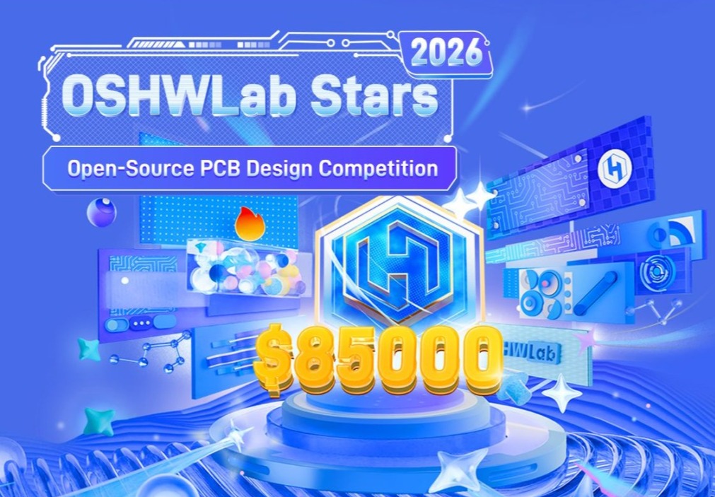
Stars2026


Activity
More
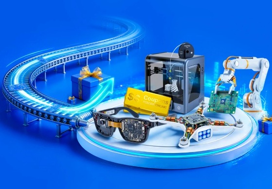
EasyEDA Spark Program (Global Hardware Creator Program) is a global initiative aimed at helping makers, engineers, students, educators and innovators turn their ideas into actual hardware projects.
EasyEDA Spark 2026
2025-12-31 ~ 2026-12-31in progress

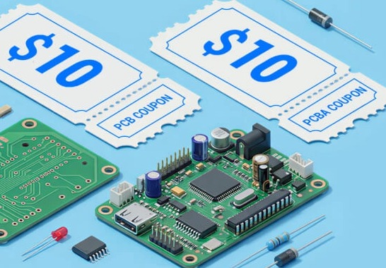
Make Your Own Christmas Gift! 🎁Join · Design · Share · Celebrate🎁 Click to [Get the coupon]
🎄 Christmas Hackathon 2025 🎅
2025-11-12 ~ 2026-01-04activity end

Open to all college and high school students majoring in electronics or enthusiasts. Preference will be given to individuals with experience in campus activities, community building, and student leadership roles.
Campus Ambassador
2024-01-01 ~ 2026-12-31in progress
Collections
More


393 project in total
Enter the Collection >
32 project in total
Enter the Collection >


Forums
MoreLibrary
How to create polygon pads with holes for a mutual capacitance switch/button footprint?
Latest Reply:
4 days agoThank you for the response. I am sorry if my explanation was not very clear.
I want to create a pad only on the top layer, but the pad has empty space inside the shape. Like this attached graphic .. the outline of a square, but not filled in. This graphic would be a single pad.
I don't want to create a through-hole in the pcb.
Thank you again.[Picture]
PCB
Need help with copper fill settings
Latest Reply:
8 days agoHello, is your question about the problem that after placing the copper pour area, the copper fill is not displayed, causing the GND not to be connected?
PCB
why my projects are not opening and says NO permission
Latest Reply:
2 days agoPlease check out this tutorial: https://prodocs.easyeda.com/en/faq/others/#what-should-i-do-if-i-have-no-permission-to-save-a-file
PCB
How do we handle DNP for ODB++ export
Latest Reply:
3 days agoFor instructions on how to exclude components from the BOM, please refer to the following tutorial:https://prodocs.easyeda.com/en/faq/schematic/#how-to-set-the-device-not-to-be-added-to-the-bom-file
Featured Articles
More Activity
Materials application instructions
Introduction: Only support "OSHWLab Stars" projects.
The order amount cannot exceed $5,000
3.0k
15
 Technique
Roll the Future: Create Smart Timer Dice
Introduction: Welcome to OSHWLab Weekly: Create, Innovate, Explore. Discover projects and master EasyEDA!
548
5
 Technique
Ordering Boards for OSHWLab Projects
Introduction: Are you new to this hobby, do you want to replicate a community project? Here's the easy way
997
6