Image

Graphing Calculator Gets USB-C Upgrade

Unlike Texas Instruments, whose graphing calculators have famously not made technological improvements in decades despite keeping the same price tag, HP has made a few more modern graphing calculators in the last few years. One of which is the HP Prime which boasts hardware from the mid-2010s including an ARM processor, a color screen, and rechargeable lithium battery. But despite this updated hardware it’s still using micro-USB for data and charging. [David] wanted to fix that by giving this calculator a USB-C port.

The first steps were disassembling the calculator case and removing the micro-USB port. The PCB is glued to the LCD screen which isn’t ideal, but he was able to work on it with everything attached. The parts are small enough to need a microscope, and with a hot air station he was quickly able to remove the USB port. His replacements from a generic online retailer were able to be soldered without much effort, but there was one major complication. The new USB-C ports didn’t account for the “On The Go” mode supported by micro-USB and were shorting a pin to ground which put the calculator into “host” mode instead of acting as a device. But using the microscope and cutting a trace on the PCB disabled this mode permanently and got the calculator working properly.

As far as modernizing calculators go, it seems like the HP Prime checks a lot of boxes, with the major downside that the LCD screen and more powerful processor means that the battery needs to be charged more often than the old TI calculators. Rather than carry a dongle around everywhere, [David] found this to be a much more efficient change to his trusty HP. If you’re still stuck using TI calculators, though, there are a few ways to modernize those as well like this build which adds a lithium battery or this one which ports a few Game Boy games to the platform.

Image

Blast Away The Flux — With Brake Cleaner?

Can you use brake cleaner for flux removal on PCBs? According to [Half Burnt Toast], yes you can. But should you? Well, that’s another matter.

In our experience, flux removal seems to be far more difficult than it should be. We’ve seen plenty of examples of a tiny drop of isopropyl alcohol and a bit of light agitation with a cotton swab being more than enough to loosen up even the nastiest baked-on flux. If we do the same thing, all we get is a gummy mess embedded with cotton fibers smeared all over the board. We might be doing something wrong, or perhaps using the wrong flux, but every time we get those results, we have to admit toying with the idea of more extreme measures.

Image
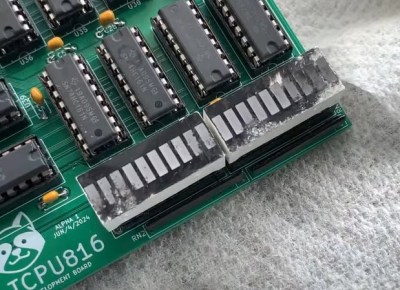
The LED bar graphs were not a fan of the brake cleaner.

[Toast] went there, busting out a fresh can of brake cleaner and hosing down some of the crustier examples in his collection. The heady dry-cleaner aroma of perchloroethylene was soon in the air, and the powerful solvent along with the high-pressure aerosol blast seemed to work wonders on flux. The board substrate, the resist layer, and the silkscreen all seemed unaffected by the solvent, and the components were left mostly intact; one LED bar graph display did a little melty, though.

So it works, but you might want to think twice about it. The chlorinated formula he used for these tests is pretty strong stuff, and isn’t even available in a lot of places. Ironically, the more environmentally friendly stuff seems like it would be even worse, loaded as it is with acetone and toluene. Whichever formula you choose, proceed with caution and use the appropriate PPE.

What even is flux, and what makes it so hard to clean? Making your own might provide some answers.

Continue reading “Blast Away The Flux — With Brake Cleaner?”

Hackaday Links Column Banner

Hackaday Links: November 17, 2024

A couple of weeks back, we covered an interesting method for prototyping PCBs using a modified CNC mill to 3D print solder onto a blank FR4 substrate. The video showing this process generated a lot of interest and no fewer than 20 tips to the Hackaday tips line, which continued to come in dribs and drabs this week. In a world where low-cost, fast-turn PCB fabs exist, the amount of effort that went into this method makes little sense, and readers certainly made that known in the comments section. Given that the blokes who pulled this off are gearheads with no hobby electronics background, it kind of made their approach a little more understandable, but it still left a ton of practical questions about how they pulled it off. And now a new video from the aptly named Bad Obsession Motorsports attempts to explain what went on behind the scenes.

Continue reading “Hackaday Links: November 17, 2024”

Image

A Brand-New Additive PCB Fab Technique?

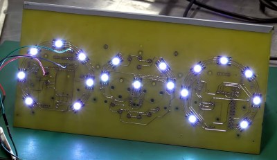
Usually when we present a project on these pages, it’s pretty cut and dried — here’s what was done, these are the technologies used, this was the result. But sometimes we run across projects that raise far more questions than they answer, such as with this printed circuit board that’s actually printed rather than made using any of the traditional methods.

Right up front we’ll admit that this video from [Bad Obsession Motorsport] is long, and what’s more, it’s part of a lengthy series of videos that document the restoration of an Austin Mini GT-Four. We haven’t watched the entire video much less any of the others in the series, so jumping into this in the middle bears some risk. We gather that the instrument cluster in the car is in need of a tune-up, prompting our users to build a PCB to hold all the instruments and indicators. Normally that’s pretty standard stuff, but jumping to the 14:00 minute mark on the video, you’ll see that these blokes took the long way around.

ImageStarting with a naked sheet of FR4 substrate, they drilled out all the holes needed for their PCB layout. Most of these holes were filled with rivets of various sizes, some to accept through-hole leads, others to act as vias to the other side of the board. Fine traces of solder were then applied to the FR4 using a modified CNC mill with the hot-end and extruder of a 3D printer added to the quill. Components were soldered to the board in more or less the typical fashion.

It looks like a brilliant piece of work, but it leaves us with a few questions. We wonder about the mechanics of this; how is the solder adhering to the FR4 well enough to be stable? Especially in a high-vibration environment like a car, it seems like the traces would peel right off the board. Indeed, at one point (27:40) they easily peel the traces back to solder in some SMD LEDs.

Also, how do you solder to solder? They seem to be using a low-temp solder and a higher temperature solder, and getting right in between the melting points. We’re used to seeing solder wet into the copper traces and flow until the joint is complete, but in our experience, without the capillary action of the copper, the surface tension of the molten solder would just form a big blob. They do mention a special “no-flux 96S solder” at 24:20; could that be the secret?

We love the idea of additive PCB manufacturing, and the process is very satisfying to watch. But we’re begging for more detail. Let us know what you think, and if you know anything more about this process, in the comments below.

Continue reading “A Brand-New Additive PCB Fab Technique?”

Image

Soldering, Up Close And Personal

A word of warning before watching this very cool video on soldering: it may make you greatly desire what appears to be a very, very expensive microscope. You’ve been warned.

Granted, most people don’t really need to get this up close and personal with their soldering, but as [Robert Feranec] points out, a close look at what’s going on when the solder melts and the flux flows can be a real eye-opener. The video starts with what might be the most esoteric soldering situation — a ball-grid array (BGA) chip. It also happens to be one of the hardest techniques to assess visually, both during reflow and afterward to check the quality of your work. While the microscope [Robert] uses, a Keyence VHX-7000 series digital scope, allows the objective to swivel around and over the subject in multiple axes and keep track of where it is while doing it, it falls short of being the X-ray vision you’d need to see much beyond the outermost rows of balls. But, being able to look in at an angle is a huge benefit, one that allows us a glimpse of the reflow process.

More after the break

Continue reading “Soldering, Up Close And Personal”

Image

Busted: Toilet Paper As Solder Wick

It didn’t take long for us to get an answer to the question nobody was asking: Can you use toilet paper as solder wick? And unsurprisingly, the answer is a resounding “No.”

Confused? If so, you probably missed our article a few days ago describing the repair of corroded card edge connectors with a bit of homebrew HASL. Granted, the process wasn’t exactly hot air solder leveling, at least not the way PCB fabs do it to protect exposed copper traces. It was more of an en masse tinning process, for which [Adrian] used a fair amount of desoldering wick to pull excess solder off the pins.

During that restoration, [Adrian] mentioned hearing that common toilet paper could be used as a cheap substitute for desoldering wick. We were skeptical but passed along the tip hoping someone would comment on it. Enter [KDawg], who took up the challenge and gave it a whirl. The video below shows attempts to tin a few pins on a similar card-edge connector and remove the excess with toilet paper. The tests are done using 63:37 lead-tin solder, plus and minus flux, and using Great Value TP in more or less the same manner you’d use desoldering braid. The results are pretty much what you’d expect, with charred toilet paper and no appreciable solder removal. The closest it comes to working is when the TP sucks up the melted flux. Stay tuned for the bonus positive control footage at the end, though; watching that legit Chemtronics braid do its thing is oddly satisfying.

So, unless there’s some trick to it, [KDawg] seems to have busted this myth. If anyone else wants to give it a try, we’ll be happy to cover it.

Continue reading “Busted: Toilet Paper As Solder Wick”

Image

Restoring A Vintage CGA Card With Homebrew HASL

Right off the bat, we’ll stipulate that what [Adrian] is doing in the video below isn’t actual hot air solder leveling. But we thought the results of his card-edge connector restoration on a CGA video card from the early 80s was pretty slick, and worth keeping in mind for other applications.

The back story is that [Adrian], of “Digital Basement” YouTube fame, came across an original IBM video card from the early days of the IBM-PC. The card was unceremoniously dumped, probably due to the badly corroded pins on the card-edge bus connector. The damage appeared to be related to a leaking battery — the corrosion had that sickly look that seems to only come from the guts of batteries — leading him to try cleaning the formerly gold-plated pins. He chose naval jelly rust remover for the job; for those unfamiliar with this product, it’s mostly phosphoric acid mixed with thickeners and is used as a rust remover.

The naval jelly certainly did the trick, but left the gold-plated pins a little worse for the wear. Getting them back to their previous state wasn’t on the table, but protecting them with a thin layer of solder was easy enough. [Adrian] used liquid rosin flux and a generous layer of 60:40 solder, which was followed by removing the excess with desoldering braid. That worked great and got the pins on both sides of the board into good shape.

[Adrian] also mentioned a friend who recommended using toilet paper to wick up excess solder, but sadly he didn’t demonstrate that method. Sounds a little sketchy, but maybe we’ll give it a try. As for making this more HASL-like, maybe heating up the excess solder with an iron and blasting the excess off with some compressed air would be worth a try.

Continue reading “Restoring A Vintage CGA Card With Homebrew HASL”