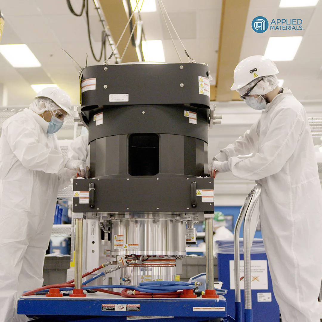
We’re proudly supporting Apple's partnership with Texas Instruments (TI) by supplying American-made chipmaking equipment to TI’s U.S. factories. #MakeItMaterialbit.ly/45jx5xt
Today, we introduced materials, technologies and systems that help chipmakers integrate chiplets into advanced 2.5D and 3D packages using hybrid bonding and TSVs. The new solutions extend Applied’s industry-leading portfolio for heterogeneous integration. bit.ly/3O6mFKj
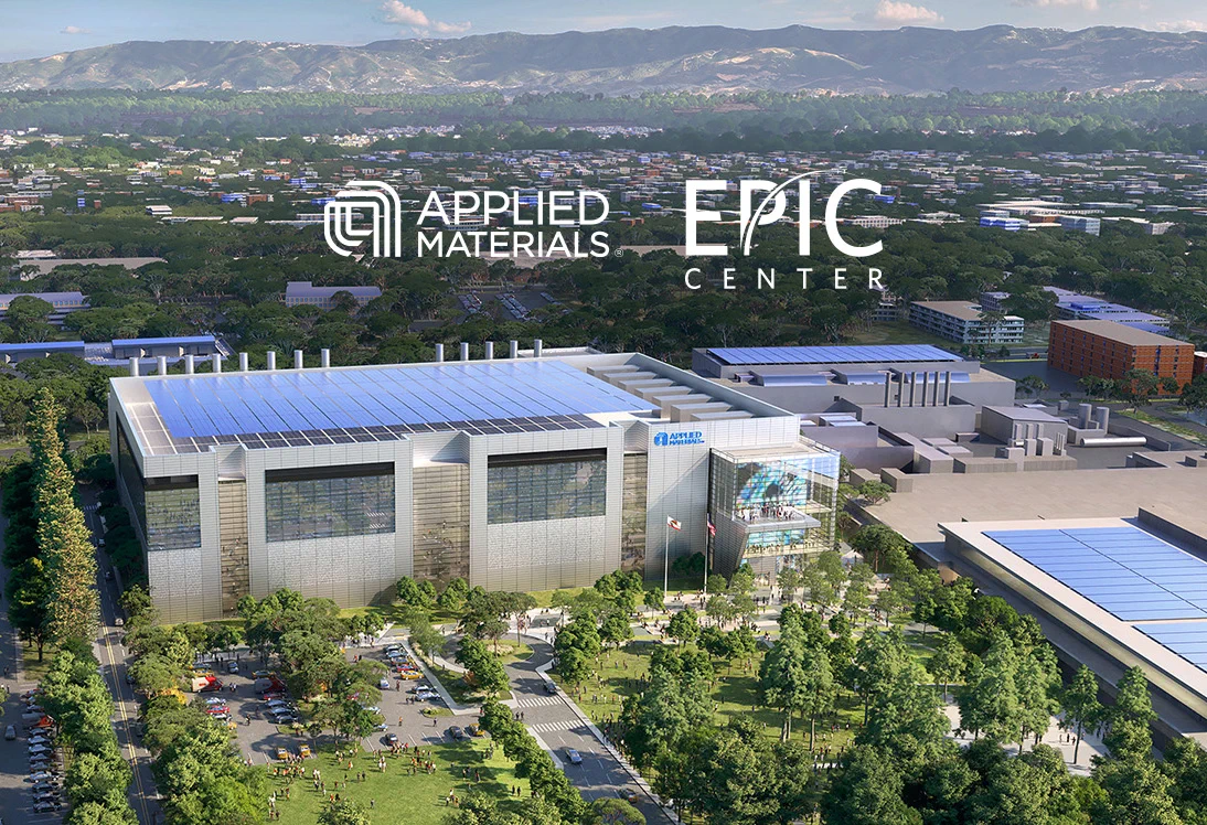
Today, we announced a landmark investment to build the world’s largest and most advanced facility for collaborative process technology and manufacturing equipment R&D. The new EPIC Center is planned as the heart of a high-velocity innovation platform. bit.ly/3q2Ty13
It was an honor to showcase our chip manufacturing systems to U.S. President Joe Biden and South Korean President Yoon Suk-yeol as they visited a Samsung fab in Korea.
Today, Applied Materials hosted Deputy Secretary of Commerce Don Graves at our Silicon Valley campus to tour the Maydan Technology Center – our state-of-the-art semiconductor R&D lab. Thank you for visiting!
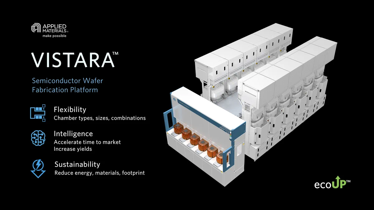
Today we introduced our most significant wafer manufacturing platform innovation in more than a decade. The new Vistara™ platform is designed to provide customers with the flexibility, intelligence & sustainability needed to tackle chipmaking challenges. bit.ly/44CzcdL
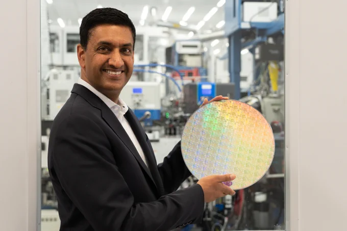
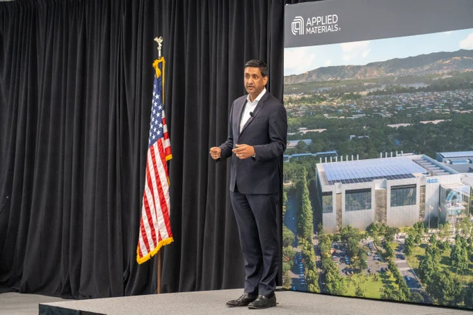
Today, Applied Materials hosted Congressman @RoKhanna at our Silicon Valley campus to speak with employees and tour the Maydan Technology Center – our state-of-the-art semiconductor R&D lab. Thank you for visiting!
Today, Applied unveiled the Sculpta patterning system: a breakthrough innovation that enables chipmakers to replace EUV double-patterning steps and reduce the cost, complexity and environmental impact of leading-edge chipmaking. Read more: bit.ly/3IZvfYR
Applied Materials looks forward to supporting Intel’s new mega-fab in Ohio and working together to build a robust semiconductor ecosystem in the Midwest. #IntelOhio#MakePossible
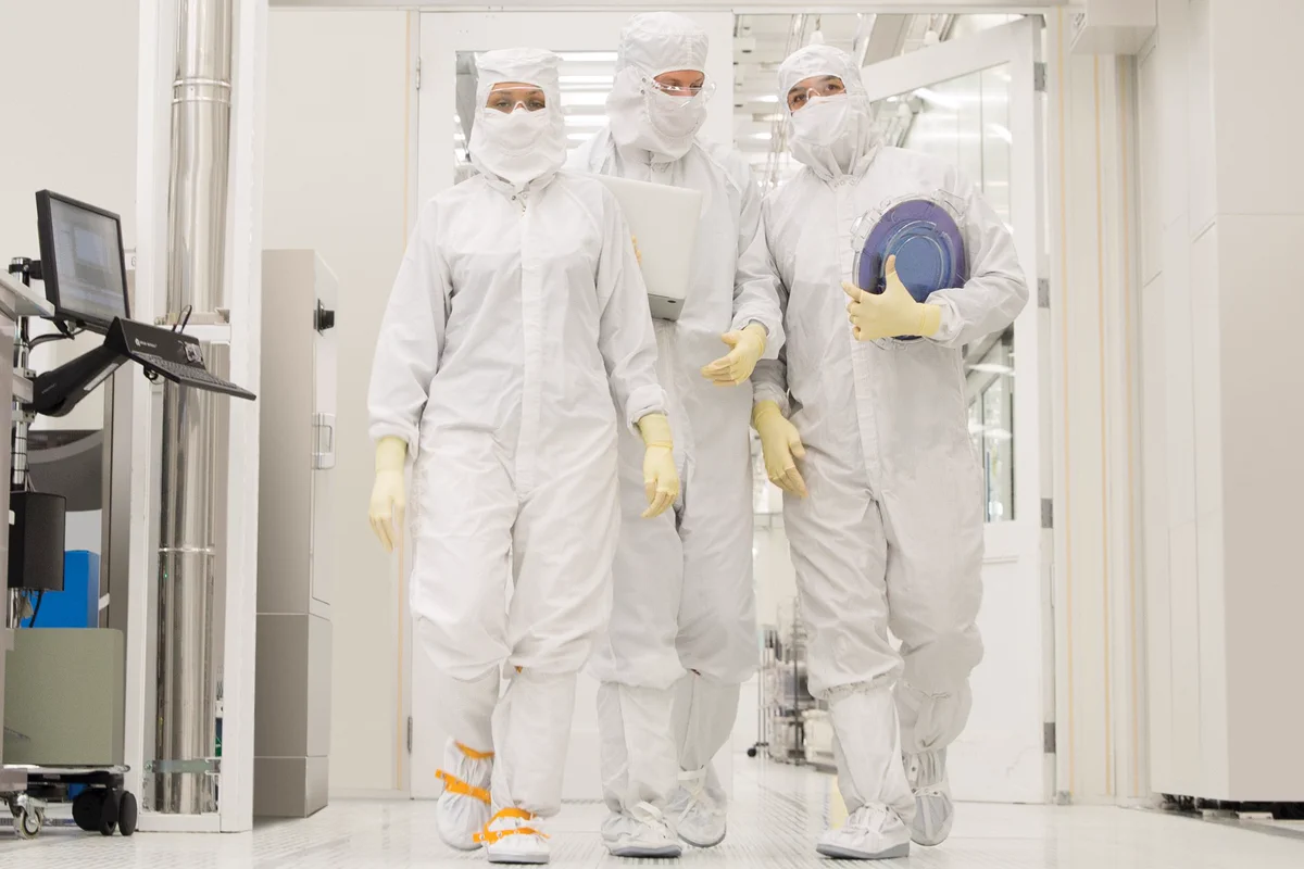
To be located in Sunnyvale, the EPIC Center is designed to provide a breadth and scale of capabilities that is unique in the chip industry, including >180,000 sq ft of state-of-the-art cleanroom for collaborative innovation with chipmakers, universities and ecosystem partners.
We are on a path to achieve 100% renewable electricity globally by 2030 and are dedicated to creating a more sustainable industry as part of our vision to #MakePossibleABetterFuture. bit.ly/3YkBw7h
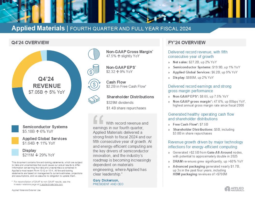
Today we reported results for the fourth quarter and full year fiscal 2024. Check out this snapshot to learn more about our financial results and business highlights.
Applied has acquired Picosun, an innovator in atomic layer deposition technology. Bringing Picosun’s talented team to Applied will strengthen our ability to help customers add more intelligence and functionality to a wide variety of edge computing devices. bit.ly/3Qs1KAs
Applied Materials celebrates President Biden signing the CHIPS and Science Act. This historic bipartisan legislation will create thousands of jobs, spur investment and fuel innovation. Applied is ready to invest and build on our foundation of manufacturing and R&D in the U.S.