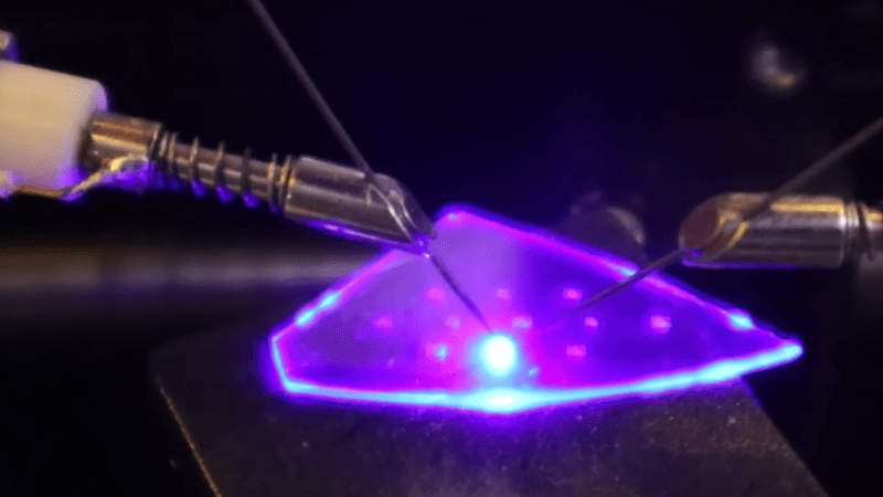
An irregular shard of a crystal wafer is set on a table, with two wire probes contacting it. Between the probes, a bright blue-purple light glows, illuminating the rest of the wafer.

Making LEDs In The Home Fab

Impressive as it most certainly is when an amateur fabricates a semiconductor, most of the projects we’ve seen are more demonstrations than workable chips. [Dr. Semiconductor], however, is going much further with his fabrication process, and is already working on a method to bond chips to printed circuit boards. It’s difficult to align a PCB with the pads on the underside of an opaque silicon wafer, however, so as a trial run he’s made and bonded some transparent LED chips.

The starting material for these chips is a gallium nitride (GaN) LED epiwafer, a stacked structure of n-doped GaN, an indium gallium nitride quantum well layer, and p-doped GaN grown on a sapphire substrate. When current passes through the structure, electrons from the n-doped layer and holes from the p-type layer recombine in the quantum well layer, emitting blue light. To make a functional LED from this, [Dr. Semiconductor] needed to make electrical contacts to both the n-type and p-type layers. Making the n-type contact required cutting through the p-type and quantum well layers.

This would normally be done with reactive ion etching in chlorine, but [Dr. Semiconductor] came up with a new process: a 355-nm ultraviolet etching laser causes GaN to break down into gallium and nitrogen, with the resulting cut being cleaned up by a potassium hydroxide etch. To deposit the contacts themselves, [Dr. Semiconductor] formed a photoresist mask, deposited metal (nickel, silver, and titanium) in a sputtering chamber, and used a developer solution to dissolve the mask and lift off the unwanted metal regions.
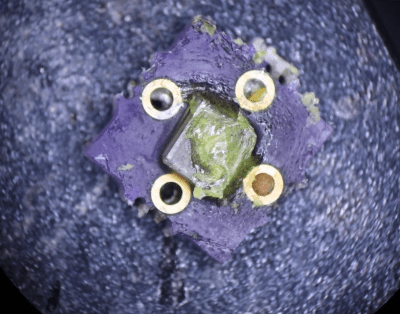
A square, purple PCB is shown under a microscope. The PCB has four vias surrounding a transparent chip, which has a blob of translucent yellow material on top of it.
The LED after bonding and phosphor application.

When [Dr. Semiconductor] applied current between the two contacts, the LED glowed bright blue. The next step was to mount it to a PCB; to do so, he first sliced the wafer into individual LED chips with the ultraviolet laser. He then electroplated indium bumps onto a printed circuit board, positioned the chip above these bumps, added some rosin flux, and melted the indium bumps. This soldered the chip to the board and let the board power the LED.

Like most commercial white LEDs, these were blue; most LED assemblies additionally include a phosphor layer which absorbs blue light and emits another color. To create a white LED, for example, [Dr. Semiconductor] mixed cerium-doped yttrium aluminium garnet phosphor powder with clear silicone and spread it over the LED. This absorbs some of the blue light and emits yellow light, and the resulting mixture of blue and yellow light looks white to human eyes.

We’ve previously covered some of the history of LEDs and the phosphors which make them useful. This seems to be the first inorganic LED we’ve seen, but we’ve also seen a few homemade OLEDs.

Thanks to [SpuriousIndices] for the tip!
Image

Electronics Near Zero

Normally, when you design an electronic gadget, you worry about how hot it will get. Automotive-grade components, for example, often have higher allowable temperatures than commercial parts. However, extremely cold environments, such as deep space or the interiors of quantum computers, are also challenging. Researchers at King Abdullah University of Science and Technology believe gallium oxide may be key to operating near absolute zero.

According to [Vishal Khandelwal], one of the researchers, most conventional electronics fail below -173C or 100K. Quantum computers routinely operate at 4K. However, β-Ga2O3 is a wide-bandgap semiconductor that has low current leakage and works at high temperatures up to 500C. However, it also avoids the freeze-out effect that traps electrons in other semiconductor materials.

Continue reading “Electronics Near Zero”

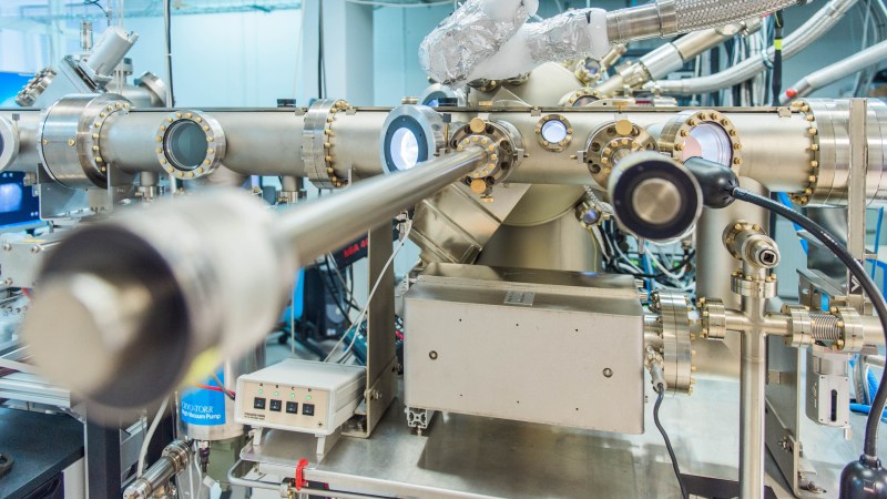
Molecular beam epitaxy system Veeco Gen II at the FZU – Institute of Physics of the Czech Academy of Sciences. The system is designed for growth of monocrystalline semiconductors, semiconducting heterostructures, materials for spintronics and other compound material systems containing Al, Ga, As, P, Mn, Cu, Si and C.

Germanium Semiconductor Made Superconductor By Gallium Doping

Over on ScienceDaily we learn that an international team of scientists have turned a common semiconductor germanium into a superconductor.

Researchers have been able to make the semiconductor germanium superconductive for the first time by incorporating gallium into its crystal lattice through the process of molecular-beam epitaxy (MBE). MBE is the same process which is used in the manufacture of semiconductor devices such as diodes and MOSFETs and it involves carefully growing crystal lattice in layers atop a substrate.

When the germanium is doped with gallium the crystalline structure, though weakened, is preserved. This allows for the structure to become superconducting when its temperature is reduced to 3.5 Kelvin. Read all about it in the team’s paper here (PDF).

It is of course wonderful that our material science capabilities continue to advance, but the breakthrough we’re really looking forward to is room-temperature superconductors, and we’re not there yet. If you’re interested in progress in superconductors you might like to read about Floquet Majorana Fermions which we covered earlier this year.

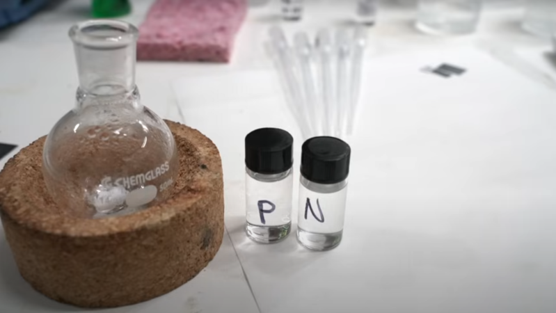
Two clear phials are shown in the foreground, next to a glass flask. One phial is labelled “P,” and the other is labelled “N”.

Designing A Hobbyist’s Semiconductor Dopant

[ProjectsInFlight] has been on a mission to make his own semiconductors for about a year now, and recently shared a major step toward that goal: homemade spin-on dopants. Doping semiconductors has traditionally been extremely expensive, requiring either ion-implantation equipment or specialized chemicals for thermal diffusion. [ProjectsInFlight] wanted to use thermal diffusion doping, but first had to formulate a cheaper dopant.

Thermal diffusion doping involves placing a source of dopant atoms (phosphorus or boron in this case) on top of the chip to be doped, heating the chip, and letting the dopant atoms diffuse into the silicon. [ProjectsInFlight] used spin-on glass doping, in which an even layer of precursor chemicals is spin-coated onto the chip. Upon heating, the precursors decompose to leave behind a protective film of glass containing the dopant atoms, which diffuse out of the glass and into the silicon.

After trying a few methods to create a glass layer, [ProjectsInFlight] settled on a composition based on tetraethyl orthosilicate, which we’ve seen used before to create synthetic opals. After finding this method, all he had to do was find the optimal reaction time, heating, pH, and reactant proportions. Several months of experimentation later, he had a working solution.

After some testing, he found that he could bring silicon wafers from their original light doping to heavy doping. This is particularly impressive when you consider that his dopant is about two orders of magnitude cheaper than similar commercial products.

Of course, after doping, you still need to remove the glass layer with an oxide etchant, which we’ve covered before. If you prefer working with lasers, we’ve also seen those used for doping. Continue reading “Designing A Hobbyist’s Semiconductor Dopant”

Image

New Bismuth Transistor Runs 40% Faster And Uses 10% Less Power

Recently in material science news from China we hear that [Hailin Peng] and his team at Peking University just made the world’s fastest transistor and it’s not made of silicon. Before we tell you about this transistor made from bismuth here’s a whirlwind tour of the history of the transistor.

The Bipolar Junction Transistor (BJT, such as NPN and PNP) was developed soon after the point-contact transistor which was developed at Bell Labs in 1947. Then after Resistor-Transistor Logic (RTL) came Transistor-Transistor Logic (TTL) made with BJTs. The problem with TTL was too much power consumption.

Continue reading “New Bismuth Transistor Runs 40% Faster And Uses 10% Less Power”

Image

Semiconductor Simulator Lets You Play IC Designer

For circuit simulation, we have always been enthralled with the Falstad simulator which is a simple, Spice-like simulator that runs in the browser. [Brandon] has a simulator, too, but it simulates semiconductor devices. With help from [Paul Falstad], that simulator also runs in the browser.

This simulator takes a little thinking and lets you build devices as you might on an IC die. The key is to use the drop-down that initially says “Interact” to select a tool. Then, the drop-down below lets you select what you are drawing, which can be a voltage source, metal, or various materials you find in semiconductor devices, like n-type or a dielectric.

It is a bit tricky, but if you check out the examples first (like this diode), it gets easier. The main page has many examples. You can even build up entire subsystems like a ring oscillator or a DRAM cell.

Designing at this level has its own quirks. For example, in the real world, you think of resistors as something you can use with great precision, and capacitors are often “sloppy.” On an IC substrate, resistors are often the sloppy component. While capacitor values might not be exact, it is very easy to get an extremely precise ratio of two capacitors because the plate size is tightly controlled. This leads to a different mindset than you are used to when designing with discrete components.

Of course, this is just a simulation, so everything can be perfect. If, for some reason, you don’t know about the Falstad simulator, check it out now.

Image

Pulsed Deposition Points A Different Path To DIY Semiconductors

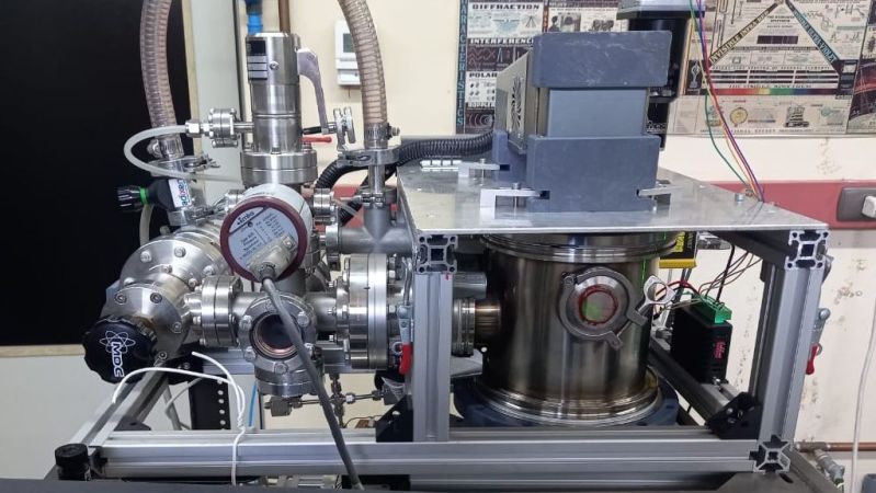
While not impossible, replicating the machines and processes of a modern semiconductor fab is a pretty steep climb for the home gamer. Sure, we’ve seen it done, but nanoscale photolithography is a demanding process that discourages the DIYer at every turn. So if you want to make semiconductors at home, it might be best to change the rules a little and give something like this pulsed laser deposition prototyping apparatus a try.

Rather than building up a semiconductor by depositing layers of material onto a silicon substrate and selectively etching features into them with photolithography, [Sebastián Elgueta]’s chips will be made by adding materials in their final shape, with no etching required. The heart of the process is a multi-material pulsed laser deposition chamber, which uses an Nd:YAG laser to ablate one of six materials held on a rotating turret, creating a plasma that can be deposited onto a silicon substrate. Layers can either be a single material or, with the turret rapidly switched between different targets, a mix of multiple materials. The chamber is also equipped with valves for admitting different gases, such as oxygen when insulating layers of metal oxides need to be deposited. To create features, a pattern etched into a continuous web of aluminum foil by a second laser is used as a mask. When a new mask is needed, a fresh area of the foil is rolled into position over the substrate; this keeps the patterns in perfect alignment.

We’ve noticed regular updates on this project, so it’s under active development. [Sebastián]’s most recent improvements to the setup have involved adding electronics inside the chamber, including a resistive heater to warm the substrate before deposition and a quartz crystal microbalance to measure the amount of material being deposited. We’re eager to see what else he comes up with, especially when those first chips roll off the line. Until then, we’ll just have to look back at some of [Sam Zeloof]’s DIY semiconductors.