Image

Decoding The NEC V20 Microcode ROM

The NEC V20 is an Intel 8088-compatible processor that features the same use of microcode, though with its own characteristics. This makes it important to use this same microcode if your goal is to create a cycle-accurate emulator of this processor, as [GloriousCow]’s goal is. Cue decoding the microcode ROM in a die shot of this CPU, in order to create a usable ROM image.

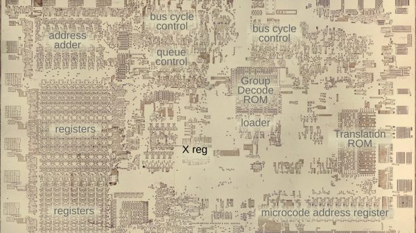
As with any fabricated ROM you can technically do it by hand, the ROM section in the die shot contained 29,928 bits which even at a pretty zippy pace would take up a considerable amount of time to parse. Here you can divide-and-conquer by handing parts of the ROM off to good friends, or you can use automation and some machine vision and theoretically get an answer as soon as you have finished writing and testing the tool.

Close-up of some of the microcode bits.

Although [Travis Goodspeed]’s MaskRomTool exists exactly to automate bit detection, it was found that there wasn’t enough contrast in the die shot for it to work reliably. What it did provide were the locations of the bits and from it 42×42 pixel PNG files of each bit.

Next a convolutional neural network (CNN) was trained to determine the difference between a 0 and 1 bit. This still took the manual classifying of 1,000 images, but seemed to work fairly well. Although some bits were marked as ambiguous, it was easy enough to use Mark 1 eyeballs to run a classification on these handful of images than to tweak the CNN model.

With this microcode in hand it was then possible to match it against the V20’s internal architecture to fully determine what each part does. Although not quite finished yet, there’s a GitHub repository containing the progress so far.

The V20’s microcode has been the focal point of much legal fighting back when NEC and Intel were still duking it out in how far one could make a CPU compatible with that of a competitor.


A blue screen is visible, with an ASCII image of the text "Hello World" is displayed.

Designing A CPU For Native BASIC

Over the years there have been a few CPUs designed to directly run a high-level programming language, the most common approach being to build a physical manifestation of a portable code virtual machine. An example might be the experimental Java processors which implemented the JVM. Similarly, in 1976 Itty Bitty Computers released an implementation of Tiny BASIC which used a simple virtual machine, and to celebrate 50 years of Tiny BASIC, [Zoltan Pekic] designed a CPU that mirrors that VM.

The CPU was created within a Digilent Anvyl board, and the VHDL file is freely available. The microcode mapping ROM was generated by a microcode compiler, also written by [Zoltan]. The original design could execute all of the 40 instructions included in the reference implementation of Tiny BASIC; later iterations extended it a bit more. To benchmark its performance, [Zoltan] set the clock rate on the development board equal to those of various other retrocomputers, then compared the times each took to calculate the prime numbers under 1000 using the same Tiny BASIC program. The BASIC CPU outperformed all of them except for Digital Microsystems’ HEX29. Continue reading “Designing A CPU For Native BASIC”

Image

This Week In Security: ClamAV, The AMD Leak, And The Unencrypted Power Grid

Cisco’s ClamAV has a heap-based buffer overflow in its OLE2 file scanning. That’s a big deal, because ClamAV is used to scan file attachments on incoming emails. All it takes to trigger the vulnerability is to send a malicious file through an email system that uses ClamAV.

The exact vulnerability is a string termination check that can fail to trigger, leading to a buffer over-read. That’s a lot better than a buffer overflow while writing to memory. That detail is why this vulnerability is strictly a Denial of Service problem. The memory read results in process termination, presumably a segfault for reading protected memory. There are Proof of Concepts (PoCs) available, but so far no reports of the vulnerability being used in the wild.
Continue reading “This Week In Security: ClamAV, The AMD Leak, And The Unencrypted Power Grid”

Image

Custom Microcode Compiler, Made In Google Sheets

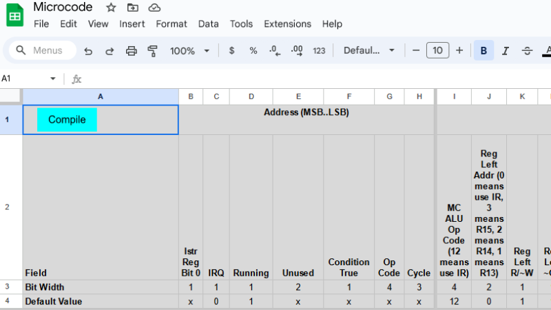
When homebrewing a CPU, one has to deal with microcode. Microcode is the low-level nuts and bolts of how, precisely, a CPU executes instructions (like opcodes) and performs functions such as updating the cycle counter or handling interrupt requests. To make this task easier, [Bob Alexander] created a microcode compiler built in Google Sheets to help with his own homebrew work, but it’s flexible and configurable enough to be useful to others, as well.

ImageA CPU’s microcode usually lives in read-only memory, and writing the microcode is only one step in the journey. [Bob]’s tool compiles his microcode into files that can be burned into memory (multiple EEPROM chips, in [Bob]’s case) or used as a Verilog program in the case of implementing the CPU in an FPGA. It’s configurable enough to be adapted for other homebrew CPU projects, though one would of course have to re-write the microcode portion.

A read-only version of the spreadsheet makes for some fun browsing, and if it piques your interest enough to get a copy of your own complete with the compiler script, you can do that here. It uses Google Sheets, and writes the output files into one’s Google Drive.

This kind of low-level project really highlights the finer points of just how the hard work of digital computing gets done. A good example is the Gigatron which implemented a RISC CPU using only microcode, memory, and logic gates in the late 70s. We’ve even seen custom microcode used to aid complex debugging.

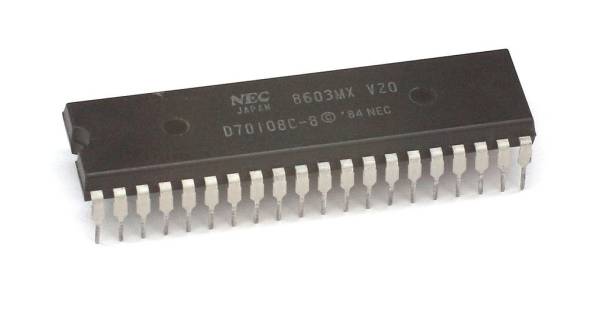
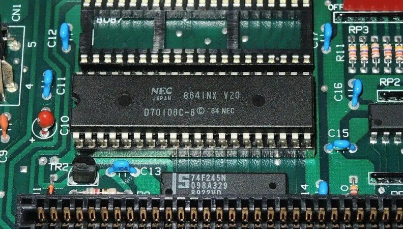
NEC V20 - Konstantin Lanzet, CC BY-SA 3.0 via Wikimedia Commons

Intel V. NEC : The Case Of The V20’s Microcode

Back in the last century, Intel saw itself faced with a need to have ‘second source’ suppliers of its 8088 and 8086 processors, which saw NEC being roped in to be one of those alternative suppliers to keep Intel’s customers happy with the μPD 8086 and μPD 8088 offerings. Yet rather than using the Intel provided design files, NEC reverse-engineered the Intel CPUs, which led to Intel suing NEC over copying the microcode that forms an integral part of the x86 architecture. In a recent The Chip Letter entry by [Babbage] this case is covered in detail.

Although this lawsuit was cleared up, and NEC licensed the microcode from Intel, this didn’t stop NEC from creating their 8086 and 8088 compatible CPUs in the form of the V30 and V20 respectively. Although these were pin- and ISA-compatible, the internal microcode was distinct from the Intel microcode due to the different internal microarchitecture. In addition the V20 and V30 also had a special 8080 mode, that provided partial compatibility with Z80 software.

Long story short, Intel sued NEC with accusations of copyright infringement of the microcode, which led to years of legal battle, which both set many precedents about what is copyrightable about microcode, and ultimately cleared NEC to keep selling the V20 and V30. Unfortunately by then the 1990s had already arrived, and sales of the NEC chips had not been brisk due to the legal issues while Intel’s new 80386 CPU had taken the market by storm. This left NEC’s x86-compatible CPUs legacy mostly in the form of legal precedents, instead of the technological achievements it had hoped for, and set the tone for the computer market of the 1990s.

Thanks to [Stephen Walters] for the tip.

Image

8086 Multiply Algorithm Gets Reverse Engineered

The 8086 has been around since 1978, so it’s pretty well understood. As the namesake of the prevalent x86 architecture, it’s often studied by those looking to learn more about microprocessors in general. To this end, [Ken Shirriff] set about reverse engineering the 8086’s multiplication algorithm.

[Ken]’s efforts were achieved by using die photos of the 8086 chip. Taken under a microscope, they can be used to map out the various functional blocks of the microprocessor. The multiplication algorithm can be nutted out by looking at the arithmetic/logic unit, or ALU. However, it’s also important to understand the role that microcode plays, too. Even as far back as 1978, designers were using microcode to simplify the control logic used in microprocessors.

[Ken] breaks down his investigation into manageable chunks, exploring how the chip achieves both 8-bit and 16-bit multiplication in detail. He covers how the numbers make their way through various instructions and registers to come out with the right result in the end.

It’s a fun look at what’s going on at the ground level in a chip that’s been around since before the personal computer revolution. For any budding chip designers, it’s a great academic exercise to follow along at home. If you’ve been doing your own digging deep into CPU architectures, don’t hesitate to drop us a line!

Image

Down The Intel Microcode Rabbit Hole

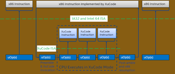
The aptly-named [chip-red-pill] team is offering you a chance to go down the Intel rabbit hole. If you learned how to build CPUs back in the 1970s, you would learn that your instruction decoder would, for example, note a register to register move and then light up one register to write to a common bus and another register to read from the common bus. These days, it isn’t that simple. In addition to compiling to an underlying instruction set, processors rarely encode instructions in hardware anymore. Instead, each instruction has microcode that causes the right things to happen at the right time. But Intel encrypts their microcode. Of course, what can be encrypted can also be decrypted.

Using vulnerabilities, you can activate an undocumented debugging mode called red unlock. This allows a microcode dump and the decryption keys are inside. The team did a paper for OffensiveCon22 on this technique and you can see a video about it, below.

Continue reading “Down The Intel Microcode Rabbit Hole”