
CONSTRUCTION NOTE / 06 COPPER LAYERS
6-Layer PCB Stackup
Define copper, core and bonding regions together. Check the thickness sum, then agree the actual material schedule with fabrication.
Open the thickness worksheet ↓ · 6-layer fabrication & quotation
L01Signal
L02Ground
L03Signal
L04Signal
L05Ground
L06Signal
Layer-role concept · not a released stackup. Physical spacing is illustrative.
STACKUP WORKSHEET
6-layer construction, in one view
Enter a proposed construction. Check its arithmetic and take the open questions to fabrication.
A matching worksheet is available from your previous page.
Choose six layers for a defined routing problem

A six-layer board is useful when the additional copper solves a named constraint: a congested escape region, a missing reference plane, a power distribution bottleneck, or separation between sensitive analog and switching circuits. Start by drawing those regions on the board outline. Count the routes that actually need a controlled reference rather than assuming that all six layers can carry signals. A plane reserved for a high-current rail is not simultaneously an unrestricted signal layer.
Compare two architectural candidates before assigning dielectric dimensions. Candidate A is signal, ground, signal, signal, ground, signal. It provides four nominal routing layers but the two middle signals can interact across their shared dielectric. Candidate B is signal, ground, power, signal, ground, signal. It provides a dedicated power layer and three signal layers. Neither is a production specification. Their usefulness depends on which gaps are thin, whether planes remain continuous, and how signals change references.
For a controller with connectors on both surfaces, identify the longest connector-to-device paths and their unavoidable transitions. For a sensor board, identify the switching-current loop and sensitive input path. The comparison should answer whether the extra internal routing layer prevents a long detour or merely creates more difficult transitions. If every channel needs two reference planes, compare an eight-layer architecture before forcing unsuitable nets into the central gap. More copper can reduce layout compromises, but it does not remove the need to document the return circuit.
A thickness calculation that does not hide the dielectric gaps

Consider an illustrative six-layer thickness budget with finished outer copper of 35 micrometres per side and inner copper of 18 micrometres on each of four layers. Copper contributes 142 micrometres. A 1.60 mm target therefore leaves 1.458 mm for dielectric if coatings are excluded from the target definition. This is arithmetic, not a recommendation for a specific laminate or press schedule.
If the two surface-to-plane gaps are each 0.12 mm, 1.218 mm remains for the three interior dielectric regions. Allocating that remainder equally would produce 0.406 mm per region, but there is no electrical reason to prefer equality. A thin power-to-ground region, a thicker middle separation, and another thin signal-to-reference gap may serve the circuit better. The fabricator must translate those requested regions into compatible available cores and bonding constructions.
Now compare a second concept with 0.18 mm outer gaps. The mechanical target is unchanged, yet the surface transmission-line geometry changes. Keeping the old trace width because both boards are called 1.6 mm six-layer boards would be a specification error. Record the layer-specific field-solver result with the accepted pressed thicknesses. Include finished conductor shape and solder-mask assumptions. An overall thickness measurement cannot establish that the internal dielectric allocation matches the model.
The downloadable schedule separates target, proposed and approved values. Blank approval cells deliberately remain blank until fabrication review; they are not automatically populated from the illustrative arithmetic.
Audit a transition as two connected paths

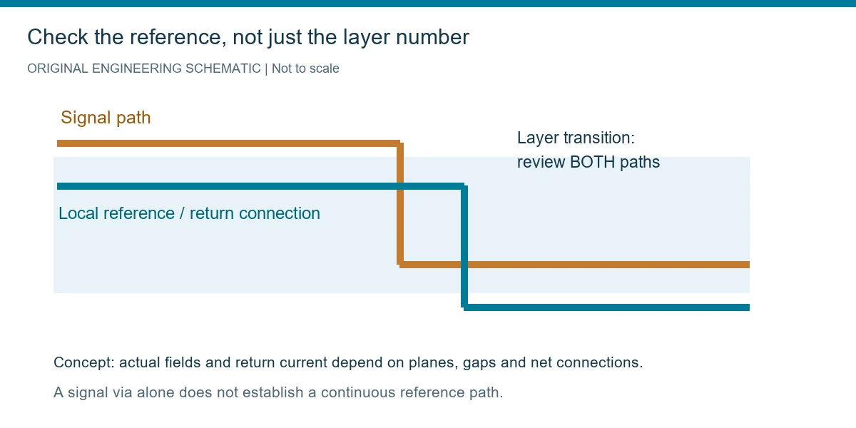
Follow a signal from its driver pad to the receiver and draw its nearby reference at every segment. When the signal moves from L1 to L6, the return must also move from the L2 reference environment to the L5 environment. A signal via by itself does not document that change. A nearby ground connection can help when both references are ground, while a change involving a power reference needs examination of the actual high-frequency return network.
Use the drill map to locate the ground connection, then check that its pads really connect to the intended planes rather than being isolated by clearances. Check connectors and mounting holes as well: a large keepout can interrupt the reference under a seemingly straight trace. A visually short route can have a poor return environment, and a longer route over uninterrupted ground can behave more predictably.
Do not approve the design from a universal maximum separation between signal and return vias. The via geometry, reference planes, signal spectrum and permitted discontinuity all matter. Use the device guidance as the first constraint, a suitable field model where required, and a representative coupon when uncertainty is material. The TI layout reference supports treating signal and return together; the decisions here are a proposed review workflow, not measured performance of this example board.
For each critical transition, capture the entering layer, leaving layer, reference pair, return connection and remaining unused barrel. This small table makes a stackup discussion much more actionable than a screenshot containing six colored stripes.
Release the stackup and routing rules as one revision

The final six-layer package should identify which dimensions are mechanical constraints and which are electrical targets. A connector may require finished board thickness within a particular range, while a controlled-impedance route needs an agreed local dielectric and conductor geometry. Distinguish those requirements so fabrication can propose a workable construction without silently changing the circuit assumptions.
Allow changes through a written comparison: original construction, proposed construction, affected net classes, updated geometry and required verification. A substitute resin system can preserve thickness while changing loss or thermal behavior. A different prepreg can preserve material family while changing pressed spacing. Neither substitution should be approved solely because the nominal layer count remains six.
Use the thickness worksheet and specialist planner output as a discussion attachment. The planning model cannot approve resin flow, copper balance, registration or electrical performance. For quotation, attach the board outline, quantities, material schedule, via spans and required records. For a repeat order, identify the approved revision rather than relying on an old email containing a preliminary table.
A useful supplier question is specific: can this reference allocation be built with available compatible materials while keeping the proposed impedance widths within the layout clearances? That question allows a constructive alternative. Asking only for the cheapest six-layer stackup leaves the engineering tradeoffs invisible. The linked fabrication page owns manufacture and quotation; this page owns the layer-allocation decision.
Choose what the central two layers should do

A conventional six-layer foil build has two inner cores and three PP bonding gaps. The middle PP lies between the two inner core assemblies, so it serves a different geometric position from the two outside PP gaps. The first candidate uses matching gaps for a transparent comparison; the row editor lets an engineer represent a proposed central thickness separately.
In signal–ground–signal–signal–ground–signal, the two central signal layers are adjacent across that middle gap. Their coupling depends on distance, routing and the reference geometry; perpendicular routes do not eliminate every interaction. If the central gap is changed, review the coupled structures rather than judging the result solely by a balanced cross-section.
A power-oriented concept changes what is routed on the middle layers and how the nearby ground plane supports the return. Before choosing between the concepts, assign the high-speed channels, current distribution and analog regions. Six is a copper-layer count, not a promise of four interchangeable signal-routing surfaces.
When comparing thin six-layer candidates, check whether the proposed trace width and clearance remain comfortable for the actual supplier process. A mechanically compact stack can create a narrow surface line for a given impedance. Send the target width range and impedance requirement with the thickness request so the fabricator can suggest a coordinated construction instead of adjusting the dielectric in isolation.
6-layer thickness, core and prepreg examples
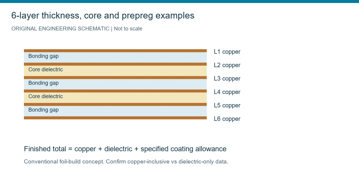
| Target | Core / substrate | Prepreg / bonding region | Calculated total | Difference |
|---|---|---|---|---|
| 0.80 mm | 2 × 0.203 mm | 3 gaps; each 1 × 1080, 65% RC | 0.800 mm | +0.000 mm |
| 1.20 mm | 2 × 0.241 mm | 3 gaps; each 3 × 10⁶, 75% RC | 1.200 mm | +0.000 mm |
| 1.60 mm | 2 × 0.533 mm | 3 gaps; each 2 × 10⁶, 75% RC | 1.592 mm | -0.008 mm |
Planning examples: 35 µm finished surface copper, 18 µm inner copper, zero separate coating allowance. These are reference candidates, not stocked or released constructions. A difference is not an approved tolerance. The tool can change the target and edit every dielectric row. Values above the FR406 reference core range are nominal design targets.
A controller needing more usable routing channels
Check the reference, not just the layer number
| Review | What to record |
|---|---|
| Reference for each critical layer | Identify the continuous plane and its dielectric spacing. |
| Transition between layers | Document the return connection and any plane change. |
| Adjacent signal layers | Check separation and coupling; orthogonal routing alone is not a guarantee. |
| Manufacturing release | Confirm pressed thickness, copper, laminate grade and agreed tolerance. |
Select the resin system, not just a Tg label
On a six-layer controller, identify the material-sensitive routes by their actual layer assignment. A top connector-to-device channel uses the L1-to-L2 region; an internal route on L4 may depend most strongly on L5 and the other nearby copper. Put those regions beside the proposed dielectric construction before deciding whether a lower-loss grade is useful. The same resin label on every row does not establish identical local geometry or propagation.
For the signal-ground-power-signal-ground-signal concept, keep the power distribution requirement on L3 separate from the impedance requirement on L4. A thinner L2-to-L3 region may support the power-reference arrangement, while the L4-to-L5 region controls a different routing task. Check how any material or pressed-thickness substitution changes these two relationships rather than evaluating only the finished 1.6 mm total.
The six-layer enquiry should therefore identify the exact grade and foil, the surface and internal controlled net classes, and which dielectric gaps are fixed by routing. If fabrication proposes another bonding construction, request the revised geometry for those named classes. Keep the accepted widths with the six-layer layout rules. A useful alternate preserves the required circuit behavior and practical escapes; a matching Tg label alone cannot demonstrate either result.
Choose the laminate and bonding system from the electrical path, assembly exposure and reliability requirements. FR-4 describes a family rather than a single dielectric constant. Glass style, resin content, frequency and the measurement method can change the value used in a circuit model. A higher Tg does not automatically mean lower insertion loss, better copper adhesion or a higher continuous service temperature.
For a routine rigid construction, identify the manufacturer and complete grade, approved thickness options and copper foil. For longer high-speed channels, compare the loss model, copper roughness and actual channel length before selecting a low-loss material. A short local bus and a long connector-to-connector route may not need the same material expenditure. Hybrid construction requires a separate bonding and compatibility review.
Keep material substitutions under engineering control. A purchasing description that says only “FR-4, high Tg” cannot preserve an impedance model or a qualification record. Ask for proposed alternatives before release, compare the required properties, and record the accepted construction in the drawing revision. Supplier data supports selection; it does not certify the finished board or establish current stock.
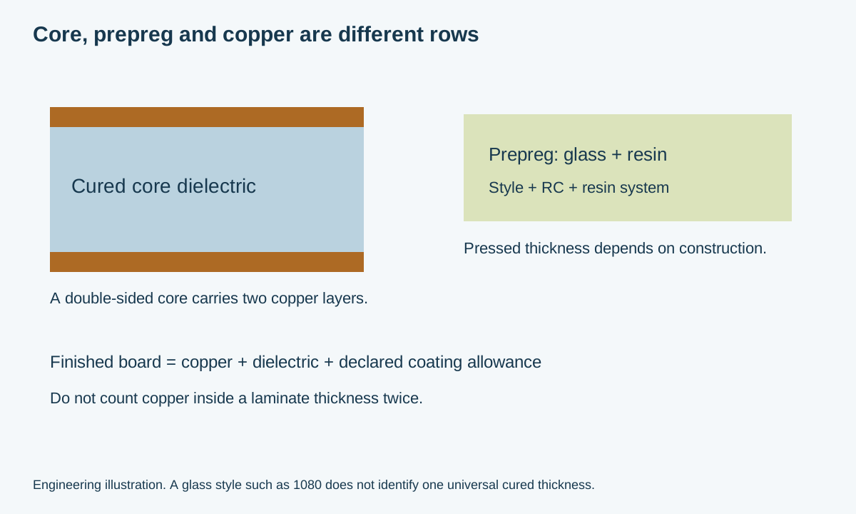
Use the right thickness in each calculation
Advanced: material-library candidates, microstrip and budget models
The existing specialist planner retains its reference construction library and model-specific controls. Its inputs are separate from the brief worksheet. Enter your intended construction and read each model’s limits before using its result.
RAYPCB ENGINEERING
Layer Engineering6 Layer PCB Stackup Planner
Loading 6 Layer PCB Stackup Planner…
Review the interconnect and inspection plan together
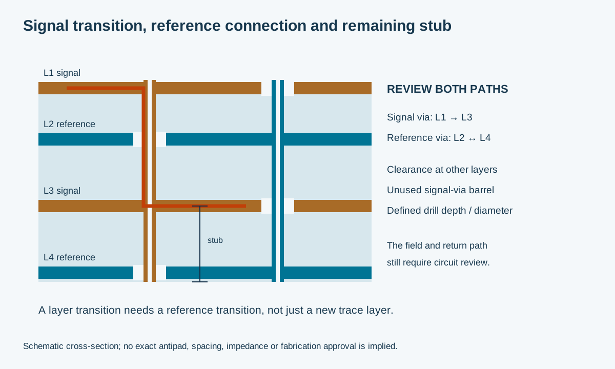
Start with a drill map that distinguishes through holes, blind holes, buried connections, microvias and any backdrill operation. Each needs a depth or layer span, diameter basis and acceptance definition. The planner’s depth-to-drill ratio is a geometric check using pre-plating drill diameter; it is not a universal plating capability limit and must not be confused with finished hole diameter.
For a conventional multilayer, inner circuits are imaged and inspected before lay-up, bonding and outer-layer processing. The required number of press cycles comes from the interconnect architecture. Additional copper layers do not automatically mean sequential lamination, stacked microvias or via-in-pad. If those features are required, include filling, capping and registration requirements in the quote scope.
Match the test to the requirement. Netlist continuity and isolation do not measure insertion loss or validate a return path. Controlled-impedance coupons need an agreed structure and test method; RF measurements need defined ports, fixtures and calibration boundaries. Dimensional inspection and relevant cross-sections should represent the actual construction and hole families. Decide which records accompany the first build and subsequent orders.
Compare complete constructions when reviewing price

Layer count is one cost driver, not a pricing formula. Material consumption, usable panel area, copper, drill families, lamination sequence, surface finish, inspection, electrical test and quantity all contribute. A narrow board can fit a panel efficiently or waste more area after process rails and coupons are included. Small quantities spread setup and fixture costs across fewer boards.
Ask comparable suppliers to quote the same material definition, finished thickness, copper, finish, hole map and acceptance scope. Separate one-time engineering or tooling from repeat fabrication. Also separate bare-board manufacture from component sourcing and assembly. A cheaper quote may simply omit a coupon, a test report or a finish requirement that another quote includes.
The optional budget uses your entered setup, fabrication-per-board and batch test allowances. It has no live factory tariff and makes no claim about current market prices. Its range is an uncalibrated planning scenario, not a statistical confidence interval. Complex and unsupported constructions produce a useful engineering brief instead of a misleading instant price. Contact remains available before any calculation.
Make the first enquiry useful, even with preliminary files
Send the board outline and mechanical requirements, fabrication artwork, drill data, quantity, intended revision and the target thickness. Include the layer order with copper weight or thickness, material grade, core and bonding-layer descriptions. Identify open decisions explicitly. A preliminary design is enough to start a review if it is clearly distinguished from a released manufacturing package.
List controlled-impedance net classes with their signal layer, reference layer, target, tolerance and intended test method. Provide the proposed via spans, finished hole sizes and any backdrill limits. For selective finishes, identify the physical regions and required deposit specification; a broad term such as gold finish does not distinguish wear contacts from solderable pads.
If assembly is included, add the BOM with manufacturer part numbers, placement data, assembly drawing and test expectations. Review connector soldering, thermal exposure and mechanical support where they affect the board. Download the current planner output and attach it with the drawing. The Contact link opens the enquiry page; it does not silently upload files or transfer calculator inputs.
Continue with the decision still open
| Next page | Use it when |
|---|---|
| Compare multilayer PCB routes | You are reconsidering the layer count. |
| 6-layer manufacturing and quote preparation | You need the fabrication scope and quote requirements. |
| Compare a 4-layer alternative | Use the same board outline, material and via constraints. |
| Compare a 8-layer alternative | Use the same board outline, material and via constraints. |
| Define controlled-impedance geometry | You need trace, reference, tolerance and coupon requirements. |
| PCB manufacturing services | Review the wider fabrication route. |
| Review thermal material requirements | Assembly exposure or reliability requirements influence the laminate. |
| Check rigid PCB manufacturing conditions | Compare the complete construction against the documented process envelope. |
6 layer PCB questions
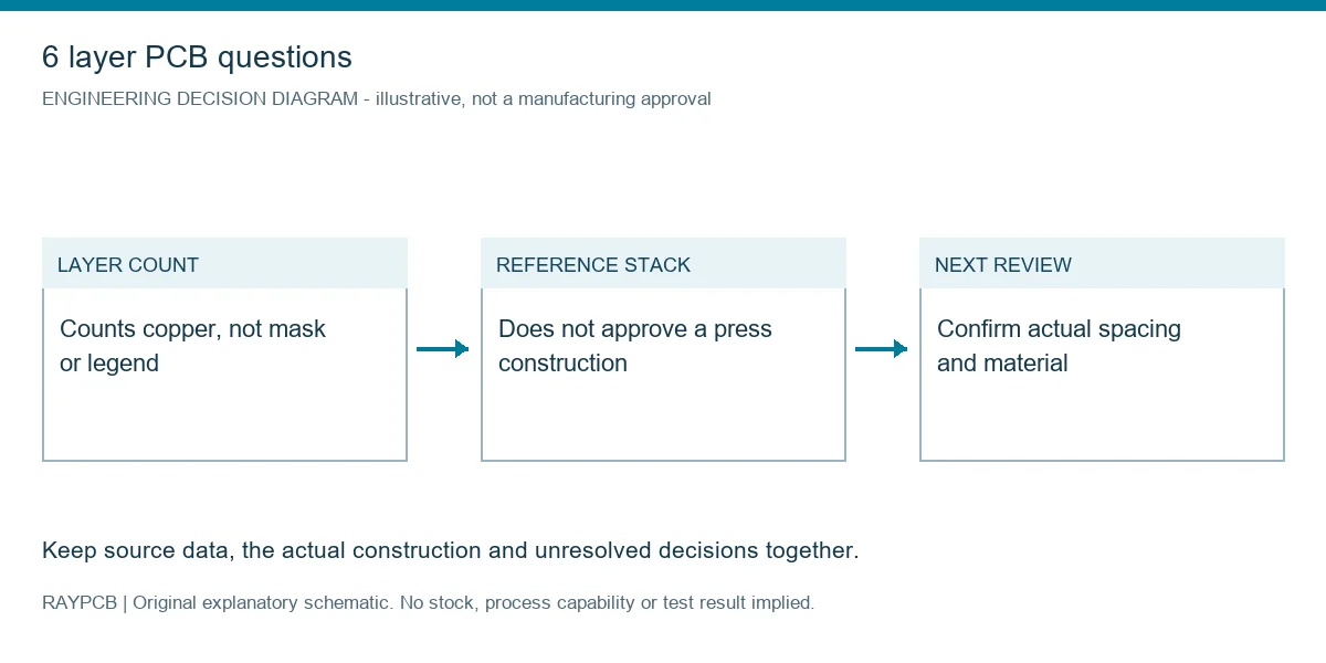
What does 6 layer PCB mean?
It counts 6 conductive copper layers. Solder mask and silkscreen do not add copper layers. The count alone does not specify the dielectric schedule, material grade, via structure or how many layers are used for signals.
Is the recommended stackup ready to manufacture?
No. It is a reference construction and thickness check. Ask the fabricator to confirm material availability, pressed dielectric values, finished copper, impedance geometry and the complete fabrication route before release.
Why does the tool show more than one thickness candidate?
Different core and PP combinations can approach the same finished thickness while changing the outer signal-to-reference gap. The best electrical and manufacturing choice is not necessarily the smallest numerical difference.
Does 2116 always have the same thickness?
No. The cloth designation alone is insufficient. Resin content, the supplied construction and the actual pressed condition matter. The reference library distinguishes entries with different resin contents and labels the original table date.
Can I get a quote without finishing the calculator?
Compare the extra routing capacity with a plane-rich arrangement and an eight-layer option for the actual net classes. Send available artwork, quantity and open questions through Contact. A useful first review can start before the final stackup is approved.
Will adding layers automatically improve signal integrity?
Only if the allocation helps the actual circuit. Poor references, split-plane crossings, unsuitable transitions and long detours can remain in a board with many layers. Review placement, routing and the return path together.
Engineering references
The linked original documents support material identification and layout principles. Use the current exact-grade and device guidance for a released project. They do not certify a RAYPCB production process.
Download the editable engineering review sheet. Complete the project-specific fields and attach it manually when requesting a review. No project files or values are automatically sent.
Engineering source context
Use the current exact-product documentation for a released design. These sources support the named principles; they do not certify a RAYPCB process.
