
PCB Manufacturing / PCB prototype
PCB Prototype Manufacturing
Get bare PCB prototypes for your own soldering or a separate assembly build. Send your board files, quantity and required date for a project-specific quote.
Already have your files? Go directly to the enquiry form. Need advice first? Send the open questions with your request.
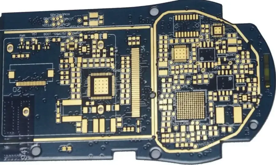
Bare PCB prototypesI will arrange the soldering and components.
Assembled PCB prototypesI need component assembly for validation.Order: bare boards; optional stencil requestRelease: Gerbers, drills and board specificationNext step: file review and project quotation
Prepare board specifications & check file names — optional
Plan Your PCB Prototype Build
Use only the sections you need. Review your summary before continuing to the enquiry form.
What happens after you send your files?
- Define the buildIdentify the file revision, quantity and delivery target. Label preliminary files and unresolved questions.
- Resolve the quotation scopeReview construction, fabrication notes, delivered format and any special test requirements.
- Approve the releaseAgree price, lead time, included checks and changes before production. Requested dates become commitments only in the confirmed order.
- Keep the next revision controlledIdentify the delivered revision and retain the agreed records. Link each design change to the files and tests it affects.
Need an NDA? Discuss it with the team before sending confidential design files. Fabrication scheduling depends on the approved release, construction, material availability and any open CAM questions.
Building the boards yourself? Plan for assembly now.
Make the prototype easy to handle and inspect
Choose individual boards or a panel to suit the assembly method. Consider stencil support, access to connectors, fiducials and tooling clearances. Keep test points accessible after the board enters its enclosure.
Hand soldering may suit accessible parts and early changes. Fine-pitch or hidden-joint packages need a process that can control solder deposition and inspect the result. An exposed pad may serve both an electrical and thermal purpose; do not assume visible lead joints prove correct attachment.
Discuss a prototype solder-paste stencil if you plan reflow. If selected packages need professional assembly, record their references and request a reviewed assembly scope.
Choose construction around the experiment
| Design need | Decisions to release | Useful engineering route |
|---|---|---|
| A simple controller or interface board | Layers, copper, finish, holes, outline and assembly format. | Keep the first build close enough to the intended product to make its test results useful. |
| Six-layer or higher routing density | Reference planes, layer order, dielectric thickness and via construction. | six-layer PCB construction and stackup planning |
| RF or controlled impedance | Exact laminate, design basis, reference planes, copper and impedance / coupon requirements. | RF material selection; controlled-impedance fabrication |
| Fine pitch or complex interconnect | Via type, sequential lamination needs and package escape geometry. | HDI design and build review |
| A moving or folded assembly | Bend use, thickness, stiffeners and mechanical envelope. | flexible PCB construction; rigid-flex planning |
A prototype made with a different material, copper construction or layer arrangement may not predict production behavior. Record intentional differences so later tests are interpreted correctly.
Release one complete fabrication package
| File / requirement | What it communicates | Review before sending |
|---|---|---|
| Copper, solder mask and silkscreen | The artwork for every intended layer. | Export from the same design revision; inspect alignment in a Gerber viewer. |
| Drill and routed features | Hole sizes, slots, plated / non-plated features and board cut-outs. | Make outline and mechanical dimensions unambiguous. |
| Fabrication drawing / stackup | Material, thickness, copper, finish and required tolerances. | Separate desired nominal values from acceptance limits. |
| Impedance / test requirements | Target nets or structures, reference planes, coupon and report needs. | Agree the stackup and test basis rather than relying on a nominal layer count. |
| Panel or individual-board request | Delivered format, break-off features and assembly interface. | Coordinate panel geometry with whoever will perform assembly. |
The ZIP tool above checks names only. Inspect the artwork and resolve CAM questions before release. General manufacturing scope is explained in the PCB manufacturing overview.
Plan the first build and the next revision together
| Use of the sample | What to record | What this does not prove |
|---|---|---|
| Incoming bare-board review | Board identity, outline, thickness and the agreed fabrication / electrical-test evidence. | That a subsequently assembled circuit works. |
| Mechanical fit | Connector locations, mounting points, keep-outs and enclosure interference. | Signal performance or thermal margin under load. |
| Assembly and first power-up | Fitted revision, polarity, design-specific safe power procedure and observations. | Long-term reliability or product certification. |
| Design change | Issue, affected board ID, root-cause evidence, changed files and approval. | That a new revision can reuse every previous validation result. |
Keep an untouched reference board where practical. Reserve separate units for destructive or external tests. After a change, identify which tests must be repeated rather than treating the next lot as automatically validated.
Control prototype cost without changing the test question
Board area is only part of the build. Layer construction, material availability, drilling, impedance requirements, panel utilization and requested schedule affect scope. Ask for separate setup, board and special-test costs when comparing offers.
Consolidating circuits into a panel can share some preparation, but rails, spacing, coupons and break-off features consume area. Do not assume that all panel area becomes delivered product. A cheaper material substitution is not equivalent if it changes the behavior you are trying to validate.
Use prototype cost guidance and a like-for-like quote comparison. For a time-sensitive release, review quick-turn PCB preparation. Move a stable design to low-volume fabrication with the approved specification and revision history.
Before you request your prototype quote
Do bare PCB prototypes include components?
No. This page plans unassembled boards. Use prototype PCB assembly when you need components sourced or fitted, and identify any customer-supplied parts.
Can I quote before all files are final?
Yes, label preliminary files and unresolved construction choices clearly. A quotation based on preliminary data is not permission to manufacture a different or unfinished release.
Does the ZIP check approve my Gerbers?
No. It reads central-directory filenames without decompressing files. It cannot inspect artwork, verify CRCs, find shorts or approve manufacturability. Review actual geometry and supplier CAM feedback.
What quantity should I order?
Start with the separate hardware, firmware, mechanical, external-test and reserve sets your team needs. Avoid counting a board twice when tests run in parallel or are destructive. The planner flags an allocation above the requested quantity.
Ready to review this build?
Send the board revision, build quantity, required date and released files. Identify unresolved design decisions and the inspection or validation work you want quoted.
Ask for the quality records relevant to your order; review quality and acceptance topics.
Engineering references
Read the Analog Devices LFCSP layout and assembly guidance for package-specific exposed-pad considerations; Ucamco Gerber format documentation for fabrication data, and Texas Instruments hardware-design resources for device-specific reference designs. Follow the exact component datasheets and approved test procedures.
