
RF PCB Materials & Design Center
Compare laminates, calculate RF geometry and define your stackup.
| Compare / grade | Dk reference | Df reference | Frequency / method | Design |
|---|---|---|---|---|
| Rogers | 3.48 Design: 3.66 | 0.0037 | 10 GHzTest conditionsProcess Dk / Df: 10 GHz, 23 °C, IPC TM-650 2.5.5.5; Design Dk: 8–40 GHz differential phase length; TCDk: −50 to 150 °C. Typical source values, not finished-board acceptance limits. Supplier source | |
| Rogers | 3.38 Design: 3.55 | 0.0027 | 10 GHzTest conditionsProcess Dk / Df: 10 GHz, 23 °C, IPC TM-650 2.5.5.5; Design Dk: 8–40 GHz differential phase length; TCDk: −50 to 150 °C. Typical source values, not finished-board acceptance limits. Supplier source | |
| Rogers | 2.2 Design: 2.2 | 0.0009 | 10 GHzTest conditionsProcess Dk / Df: 10 GHz, 23 °C, IPC TM-650 2.5.5.5; Design Dk: 8–40 GHz differential phase length; TCDk: −50 to 150 °C. Typical source values, not finished-board acceptance limits. Supplier source | |
| Rogers | 2.33 Design: 2.33 | 0.0012 | 10 GHzTest conditionsProcess Dk / Df: 10 GHz, 23 °C, IPC TM-650 2.5.5.5; Design Dk: 8–40 GHz differential phase length; TCDk: −50 to 150 °C. Typical source values, not finished-board acceptance limits. Supplier source | |
| Rogers | 6.15 Design: 6.5 | 0.002 | 10 GHzTest conditionsProcess Dk / Df: 10 GHz, 23 °C, IPC TM-650 2.5.5.5; Design Dk: 8–40 GHz differential phase length; TCDk: −50 to 150 °C. Typical source values, not finished-board acceptance limits. Supplier source | |
| Rogers | 10.2 Design: 11.2 | 0.0022 | 10 GHzTest conditionsProcess Dk / Df: 10 GHz, 23 °C, IPC TM-650 2.5.5.5; Design Dk: 8–40 GHz differential phase length; TCDk: −50 to 150 °C. Typical source values, not finished-board acceptance limits. Supplier source | |
| Rogers | 3.48 Design: 3.66 | 0.0037 | 10 GHzTest conditionsProcess Dk / Df: 10 GHz, 23 °C, IPC TM-650 2.5.5.5; Design Dk: 8–40 GHz differential phase length; TCDk: −50 to 150 °C. Typical source values, not finished-board acceptance limits. Supplier source | |
| AGC | 3 Design: not populated | 0.0013 | See sourceTest conditionsPublished selector values; frequency, test method and design-Dk basis are not specified in this selector. Confirm the exact grade datasheet before design. Supplier source | |
| AGC | 10.2 Design: not populated | 0.0025 | See sourceTest conditionsPublished selector values; frequency, test method and design-Dk basis are not specified in this selector. Confirm the exact grade datasheet before design. Supplier source | |
| AGC | 2.97 Design: not populated | 0.002 | See sourceTest conditionsPublished selector values; frequency, test method and design-Dk basis are not specified in this selector. Confirm the exact grade datasheet before design. Supplier source | |
| AGC | 3.5 Design: not populated | 0.0007 | See sourceTest conditionsPublished selector values; frequency, test method and design-Dk basis are not specified in this selector. Confirm the exact grade datasheet before design. Supplier source | |
| AGC | 3.5 Design: not populated | 0.002 | See sourceTest conditionsPublished selector values; frequency, test method and design-Dk basis are not specified in this selector. Confirm the exact grade datasheet before design. Supplier source | |
| AGC | 6.15 Design: not populated | 0.002 | See sourceTest conditionsPublished selector values; frequency, test method and design-Dk basis are not specified in this selector. Confirm the exact grade datasheet before design. Supplier source | |
| AGC | 3.5 Design: not populated | 0.0026 | See sourceTest conditionsPublished selector values; frequency, test method and design-Dk basis are not specified in this selector. Confirm the exact grade datasheet before design. Supplier source | |
| AGC | 2.55 Design: not populated | 0.0018 | See sourceTest conditionsPublished selector values; frequency, test method and design-Dk basis are not specified in this selector. Confirm the exact grade datasheet before design. Supplier source | |
| AGC | 2.2 Design: not populated | 0.0009 | See sourceTest conditionsPublished selector values; frequency, test method and design-Dk basis are not specified in this selector. Confirm the exact grade datasheet before design. Supplier source | |
| AGC | 3 Design: not populated | 0.0014 | See sourceTest conditionsPublished selector values; frequency, test method and design-Dk basis are not specified in this selector. Confirm the exact grade datasheet before design. Supplier source | |
| Isola | 3 Design: not populated | 0.0017 | 2 / 10 GHzTest conditionsDk at 2/10 GHz: IPC 2.5.5.5; Df at 2/10 GHz: Bereskin Stripline. Supplier typical data; no separate design Dk populated. Supplier source | |
| Ventec | 6.15 Design: 6.45 | 0.0025 | 10 GHzTest conditionsProcess Dk and Df: IPC 2.5.5.5 at 10 GHz. Design Dk: differential phase length at 8–40 GHz. Supplier source | |
| Shengyi | 3.42 Design: not populated | 0.003 | 10 GHzTest conditionsDk 3.42: IPC 2.5.5.5 at 10 GHz, Z direction. Other methods give different values; use the source construction. Df: supplier RF selector value. Supplier source | |
| Panasonic | 3.31 Design: not populated | 0.0023 | 14 GHzTest conditions2022 MEGTRON7 sheet: typical Dk/Df at 14 GHz. Exact construction, glass and foil must be matched; no separate design Dk populated. Supplier source |
Compare selected candidates
Different test methods and frequencies are not equivalent measurements. No automatic best-material ranking is produced. Missing data stays unresolved.
Use the material as an explicit model input
· Open supplier source · Material family guide
Review reference conditions before using a material value.
Signal conductor W · local dielectric h · continuous reference plane
Cross-section concept; GCPW also needs connected lateral grounds.
Cross-section concept; GCPW also needs connected lateral grounds.
Explore impedance tolerance corners
Estimate the dielectric contribution to loss
Define the construction layer by layer
Creating a new stack replaces the worksheet rows. Blank dielectrics stay unresolved. The first core uses your selected material and local design height.
Transfer requires an RF signal on L1, the selected material as one core, and L2 ground. A thickness sum does not approve lamination, copper balance or via reliability.
For a six-layer project, review six-layer stackup choices and six-layer PCB fabrication requirements.
Choose the engineering question you need to answer
Antenna · rectangular patch starting dimensions
Uses the current line-design Dk and local h. This is a thin-substrate starting geometry; feed, ground size, enclosure, bandwidth and radiation pattern require EM validation.
Radar / array feed · phase mismatch
Use effective permittivity from an appropriate model or measurement at the operating band. Do not substitute laminate Dk automatically.
RF amplifier · DC / RF power balance
Use consistent measurement planes. Dissipation = DC input + RF input − RF output. Drain efficiency and power-added efficiency use different numerators.
Divider / termination · embedded resistor geometry
Budget the build scope, then request a reviewed quote
The brief contains current inputs and current calculated results. Incomplete decisions are welcome. Contact opens the enquiry page; parameters and files are not automatically transferred. Attach the downloaded brief with your design files. Nothing is sent by this workbench.
Generate a brief after making your selections.
Choose the material role before comparing a brand
An RF PCB controls the signal path through its laminate, copper, reference planes and transitions. A low Df cannot compensate for an unsuitable return path. Compare complete constructions and retain the conditions behind every value.
| Material route | What to specify |
|---|---|
| Rogers | RF laminates and bonding systems |
| Arlon | Exact grade and current supplier mapping; AD series is in Rogers’ current catalogue |
| AGC / Taconic | RF laminate families and grade-specific constructions |
| Isola | RF and low-loss multilayer constructions |
| Panasonic / MEGTRON | MEGTRON is a Panasonic series; specify the full product code and glass/foil construction |
| Ventec | RF thermoset and PTFE systems; identify the exact grade |
| Shengyi | Named RF/microwave grades, distinct from general-purpose FR-4 |
| Qnity | Pyralux and flexible material systems; retain the exact laminate/bondply identity |
| Sheldahl | Flexible films and composite construction roles |
| Ohmega Ticer | Resistive foil: sheet resistance, geometry and integration |
| Tatsuta | Shielding films, grounding and construction |
| Evonik / ROHACELL HF | Antenna/radome foam core. Compare as a structural dielectric, not as a copper-clad laminate. |
| ThinFlex | Low-Dk/Df flexible copper-clad systems. Confirm grade, film, adhesive and test conditions. |
For other established routes, see PTFE-based PCB constructions, Nelco material specifications and legacy DuPont material identifiers. These are material routes, not automatic substitutes.
Keep the source conditions with the number
Process Dk, design Dk and construction-specific values answer different questions. Do not rank measurements taken at different frequencies or by different methods as if they were identical. Missing thickness, foil or bonding information remains an open decision.
Read the material references without using the tool
| Reference grade | Dk / design Dk | Df | Source conditions |
|---|---|---|---|
| RO4350B | 3.48 / 3.66 | 0.0037 | Process Dk / Df: 10 GHz, 23 °C, IPC TM-650 2.5.5.5; Design Dk: 8–40 GHz differential phase length; TCDk: −50 to 150 °C. Typical source values, not finished-board acceptance limits. Supplier reference |
| RO4003C | 3.38 / 3.55 | 0.0027 | Process Dk / Df: 10 GHz, 23 °C, IPC TM-650 2.5.5.5; Design Dk: 8–40 GHz differential phase length; TCDk: −50 to 150 °C. Typical source values, not finished-board acceptance limits. Supplier reference |
| RT/duroid 5880 | 2.2 / 2.2 | 0.0009 | Process Dk / Df: 10 GHz, 23 °C, IPC TM-650 2.5.5.5; Design Dk: 8–40 GHz differential phase length; TCDk: −50 to 150 °C. Typical source values, not finished-board acceptance limits. Supplier reference |
| RT/duroid 5870 | 2.33 / 2.33 | 0.0012 | Process Dk / Df: 10 GHz, 23 °C, IPC TM-650 2.5.5.5; Design Dk: 8–40 GHz differential phase length; TCDk: −50 to 150 °C. Typical source values, not finished-board acceptance limits. Supplier reference |
| RO3006 | 6.15 / 6.5 | 0.002 | Process Dk / Df: 10 GHz, 23 °C, IPC TM-650 2.5.5.5; Design Dk: 8–40 GHz differential phase length; TCDk: −50 to 150 °C. Typical source values, not finished-board acceptance limits. Supplier reference |
| RO3010 | 10.2 / 11.2 | 0.0022 | Process Dk / Df: 10 GHz, 23 °C, IPC TM-650 2.5.5.5; Design Dk: 8–40 GHz differential phase length; TCDk: −50 to 150 °C. Typical source values, not finished-board acceptance limits. Supplier reference |
| RO4835 | 3.48 / 3.66 | 0.0037 | Process Dk / Df: 10 GHz, 23 °C, IPC TM-650 2.5.5.5; Design Dk: 8–40 GHz differential phase length; TCDk: −50 to 150 °C. Typical source values, not finished-board acceptance limits. Supplier reference |
| Astra MT77 | 3 / not populated | 0.0017 | Dk at 2/10 GHz: IPC 2.5.5.5; Df at 2/10 GHz: Bereskin Stripline. Supplier typical data; no separate design Dk populated. Supplier reference |
| VT-6706 | 6.15 / 6.45 | 0.0025 | Process Dk and Df: IPC 2.5.5.5 at 10 GHz. Design Dk: differential phase length at 8–40 GHz. Supplier reference |
| S7136H | 3.42 / not populated | 0.003 | Dk 3.42: IPC 2.5.5.5 at 10 GHz, Z direction. Other methods give different values; use the source construction. Df: supplier RF selector value. Supplier reference |
| MEGTRON7 R-5785(N) | 3.31 / not populated | 0.0023 | 2022 MEGTRON7 sheet: typical Dk/Df at 14 GHz. Exact construction, glass and foil must be matched; no separate design Dk populated. Supplier reference |
References checked 17 October 2026. Typical supplier values are not finished-board acceptance limits or stock statements. Rogers catalogue materials and thicknesses can be sourced; confirm foil combinations and the order schedule. Other sources require project-specific procurement confirmation. Read the high-frequency material purchasing checklist for the full release specification.
Use an application question to guide the next calculation
| Application | Design question | Useful next check |
|---|---|---|
| Antenna | What changes when dielectric thickness or Dk changes? | Compare patch seed dimensions, feed geometry and tolerance; verify the complete antenna with EM simulation. |
| Radar / array | How much path mismatch consumes the phase budget? | Record band, reference planes, effective permittivity and transitions; agree fixtures and de-embedding. |
| Power amplifier | Where does the DC and RF input power go? | Separate device dissipation, board thermal path, matching and bias isolation. |
| Receiver / LNA | How much loss occurs ahead of the first gain stage? | Track input loss, matching, temperature assumptions, shielding and supply isolation. |
| Filter / divider | Which etched features dominate tuning and tolerance? | Review coupling gaps, resonant lengths, embedded resistance and measurement access. |
| RF flex | What is the complete bent and shielded construction? | Include adhesive, coverlay, shields, bending state and terminations; core-film Dk alone is insufficient. |
Three engineering examples you can reproduce
Calculated scenarios and review exercises · not measured customer projects
5.8 GHz patch antenna: compare a design starting point
Use Dk 3.66 and a local dielectric height of 0.254 mm in RF geometry, then set 5.8 GHz in Application checks. The patch tool returns initial rectangular dimensions. Change one input to see its effect; feed position, finite ground, housing and the radiation pattern still need simulation and prototype tuning.
77 GHz radar feed: translate phase budget into a length allowance
With an explicitly assumed effective permittivity of 2.8, compare a 0.05 mm route difference against a 5° phase allowance. The phase worksheet handles electrical length only; it does not validate laminate loss, dispersion or a 77 GHz launch.
RF power amplifier: separate efficiency from the thermal problem
Enter 40 W DC input, 1 W RF input and 20 W RF output. Device power balance gives 21 W dissipation, 50% drain efficiency and 47.5% PAE. A thermal solution then needs package, interface, board and cooling boundary conditions; material thermal conductivity alone cannot predict junction temperature.
From a proposed RF stack to an inspectable board
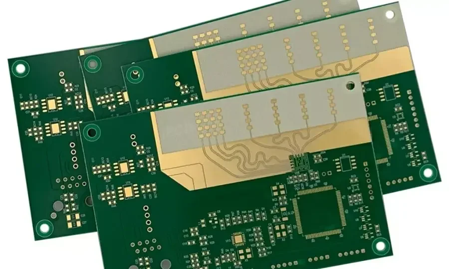
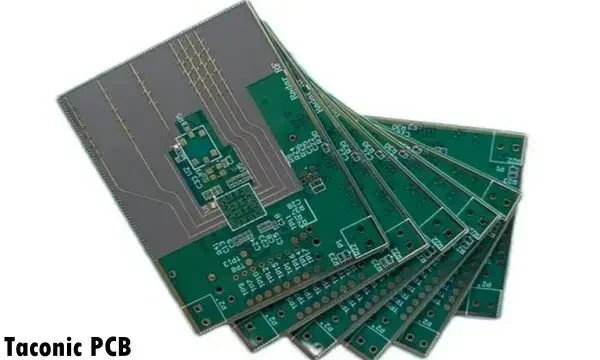
| Decision | Define before release |
|---|---|
| Reference plane and hybrid structure | Identify RF layers, dielectric heights, pressed bonding layers, copper balance and lamination compatibility. |
| Launches, vias and edges | Provide connector data, pads/antipads, return vias, stubs, cavities and controlled edge dimensions. |
| Finish and solder mask | State exposed RF areas, finish, mask openings and any coatings included in the simulation. |
| Material changes | Require approval for substitutions that alter model data, foil, bonding or mechanical behaviour. |
Review Rogers mixed-stack planning for that material route, or multilayer PCB construction for the broader build. The PCB manufacturing workflow connects the released drawing to fabrication scope.
Electrical continuity is not RF acceptance
| Verification | Specify explicitly |
|---|---|
| Bare-board electrical test | Connectivity, isolation and required records. |
| Impedance coupon | Geometry, tolerance, method and reporting; agree its relevance to the actual routes. |
| VNA measurement | Sweep, calibration, de-embedding, reference planes, fixtures, limits and sample versus every-board scope. |
| Traceability and dimensions | Material identification, construction and critical feature measurements. |
RF tests and fixtures require project-specific agreement. Request relevant quality records and review manufacturing equipment against the proposed work. No unprovided customer reports or measured performance are implied by the example tools.
RF PCB design and purchasing questions
Can FR-4 be used for an RF circuit?
It depends on path length, loss and phase budgets, variation and test requirements. There is no single frequency boundary that approves all FR-4 or requires every design to use PTFE.
Is the lowest Df always the best choice?
No. Compare the measured conditions, copper, geometry, thermal behaviour, processing and available constructions. A nominal value is one part of a build decision.
Can RF and digital layers share a board?
Yes, a hybrid is a construction to review. Identify RF reference planes, the complete bonding system and every layer transition; total board thickness alone is insufficient.
What is the minimum order or guaranteed delivery time?
Confirm quantity, exact construction and required date with the project quotation. The material directory is not a stock or lead-time promise.
Does the tool submit my files or approve the design?
No. It runs locally in the browser and downloads a planning brief. Attach it with released fabrication data on Contact. Calculations do not approve manufacturability.
Why can a quotation change after file review?
The actual foil, panel utilization, lamination, via work, mask/finish, tolerances and test scope can differ from initial assumptions. Compare quotations for the same released construction.
Model references and a useful next step
Microstrip and grounded CPW use documented quasi-static approximations with geometry guards. Symmetric stripline is a zero-thickness reference. Finite grounds, frequency dispersion, roughness, masks, connectors and transitions need an appropriate field solver. The patch model provides starting dimensions; it does not predict measured gain or bandwidth.
For a deeper loss and phase review, use high-frequency PCB design guidance. For populated RF boards, define the assembly and component-sourcing scope.
Send the requirements with the files
Include fabrication and drill files, board revision, quantity, material/foil/stackup, impedances, mask/finish, RF acceptance scope and requested delivery. Early-stage enquiries can identify open decisions instead of guessing missing requirements.
Request an RF PCB Quote