
RAYPCB · Flexible circuit engineering & manufacture
Flex PCB Stackup Design & Thickness Planning
Document the physical layers in each region.
Prepare a top-to-bottom flexible PCB stackup, compare regional thickness intervals and record the drawing basis.
Bending zoneCoverlay + adhesiveCopper / PI / copperAdhesive + coverlay
Contact zoneExposed contact + finishRegional flex constructionLocal bond + stiffener
Illustrative two-layer regions, not to scale. Define the actual layers and contact side from the drawing.
Choose what you need to resolve
Use a check below, or send existing files directly. You do not need to finish the worksheet to enquire.
Build and compare regional stackups
Use only the checks your project needs. Already have files? Send your files directly for a quote.
No data is sent by this worksheet.
Carry Brief to Enquiry temporarily keeps this text in the same browser tab and adds it to the Contact message. Review it there and attach your actual files. No request is submitted until you send the form.
Project inputs stay in this tab. Carrying a brief uses temporary tab storage for up to 30 minutes; files are not transferred. Examples explain arithmetic and are not approved production stackups.
Keep the regions and their evidence together
The constituent worksheet calculates one physical region at a time. Save one candidate, then enter the next region or architecture. Each list must name its material/drawing source and actual copper count. A support layer in a connector region is not part of the bending-zone thickness.
Worst-case arithmetic adds the individual allowances; it does not establish finished thickness after pressing, local plating, adhesive movement or surface treatment. Agree the measured quantity and the measurement location with the fabricator.
Map the regions before adding layer thicknesses

Begin with a flat outline and assign region identifiers. A simple flex could have F1 for the free span, C1 for a connector tail and S1 for a component support. The same conductor may pass through all three, while coverlay openings, stiffeners and adhesive layers change locally. A single overall thickness callout can obscure these differences and create an inspection requirement that is impossible to interpret consistently.
For each region, state the task that controls thickness. In the free span it may be bend behavior or package clearance. At an insertion tail it is often the connector's mating window. Under a component it may be assembly support or coplanarity. If controlled impedance is required, identify the signal and reference layers in that region and the relevant dielectric separation. A mechanical total thickness is not the same input as the spacing between a signal conductor and its reference.
Use the regional map to distinguish a uniform flex from a deliberately varying construction. Local reinforcement is not another conductive layer, and an exposed contact window does not retain coverlay simply because coverlay exists elsewhere on the sheet. Mark the measurement cross-section so a reviewer can see exactly what is counted. The Flex manufacturing hub remains the route for selecting the overall build; this page supports the more specific task of documenting its layers. Once regions are defined, thickness questions become answerable: which local stack is too thick, which interface fixes the limit, and which layers may change? That prevents an electrical optimization in one area from quietly breaking a mechanical interface in another.
What belongs in a flex PCB stackup?
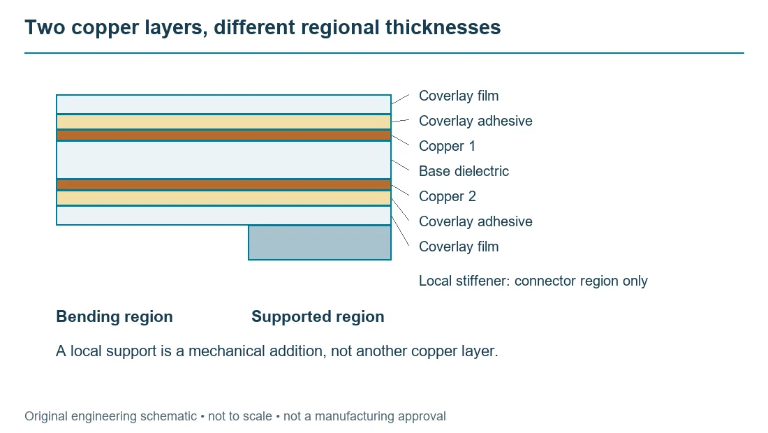
A flex PCB stackup identifies every conductive and insulating layer, their order, material designation and thickness in a defined region. Copper-layer count is only one part of that description. A two-layer flex circuit can contain two copper layers, one base film and separate coverlay film and adhesive on both sides. A local connector stiffener adds another regional construction without adding an electrical layer. Start with the region that actually bends, then document contact fingers, component support and any other local additions separately.
This page addresses pure flexible circuits. A bonded support sheet does not automatically turn a flex into a multilayer rigid-flex board with plated interconnections through rigid sections. If your drawing integrates electrically active rigid regions, use the rigid-flex stackup guide for regional layer mapping. For fabrication scope and a supplier review, the flexible PCB manufacturing page remains the commercial starting point. The worksheet above helps prepare a construction proposal; it does not select available stock or approve bend life.
Read the construction one physical layer at a time
| Stackup entry | What to specify | What it does not tell you alone |
|---|---|---|
| Copper | Foil type, nominal starting thickness and finished requirement | Finished conductor profile, plating distribution or endurance |
| Base polyimide | Exact laminate and dielectric thickness | Total circuit thickness or universal thermal rating |
| Laminate adhesive | Grade and intended finished bondline, if present | The separate coverlay or stiffener bondline |
| Coverlay film | Material, thickness, side and openings | Adhesive flow into etched spaces |
| Coverlay adhesive | Material and thickness basis | Guaranteed finished height above every feature |
| Bonding layer | Exact material and regional extent | Whether a multilayer section may repeatedly flex |
| Local stiffener | Side, outline, material and bondline | An extra signal layer or a universal connector fit |
An adhesiveless copper-clad laminate removes the separate adhesive interface from that laminate construction. It does not mean the complete finished circuit contains no adhesive. Coverlay, multilayer bonding and support attachment may still introduce bondlines. The Pyralux AP manufacturer product information identifies an adhesiveless, double-sided all-polyimide laminate family. Its construction options are material data, not a ready-to-order RAYPCB finished stackup.
Keep a separate row for every real constituent rather than entering a combined “polyimide thickness” that hides adhesive. Distinguish purchased sheet values from expected pressed values and from measured acceptance limits. Etched copper coverage, adhesive flow and pressing conditions can change the final local section. A useful drawing therefore names the measurement region and identifies which thickness values still require the fabricator's confirmation.

Distinguish adhesive-based and adhesiveless laminate structures

An adhesiveless copper-clad laminate removes the separate base adhesive layer from that particular laminate construction. It does not mean the completed board contains no adhesive. Coverlay, bonding between substructures and reinforcement can still introduce adhesive. A drawing that says “adhesiveless flex” without a layer table can therefore conceal important contributions to the final thickness and process behavior.
An adhesive-based laminate includes the film, bonding layer and copper as a defined product construction. For either route, specify the relevant material product and copper option rather than inventing a stack from individually convenient dimensions. A supplier's catalogue identifies available constructions; it does not establish that every mathematical combination is a standard purchase item. If a nonstandard combination is needed, treat availability, lead time and process review as explicit questions.
For an illustrative single-layer span, a nominal stack might comprise 25 micrometres of base film, 18 micrometres of copper, 25 micrometres of coverlay adhesive and 12.5 micrometres of coverlay film. The arithmetic sum is 80.5 micrometres. Adding a hypothetical 12.5 micrometre base adhesive contribution changes that nominal sum to 93 micrometres. This comparison only demonstrates bookkeeping; it does not compare qualified materials or predict which build will last longer. Real adhesive distribution around copper and processing variation must still be addressed. Keep the material description and the thickness calculation together so a change of laminate cannot preserve an obsolete total. Also distinguish starting copper from additional plated copper where that process is present; calling both “half-ounce copper” may omit a significant finished contribution.
Pyralux AP is an example of an adhesiveless all-polyimide laminate. The protective and bonding layers in a finished board still need their own specification.
Three stackup architectures and one worked sum
A single-sided construction places one patterned copper layer on a flexible dielectric. Protection on the circuit side and access to the other side depend on the design. A two-sided construction places copper on both sides of a base dielectric, with plated connections where specified and coverlay openings where access is needed. A multilayer flex joins sub-constructions with bonding material. Increasing the number of copper layers does not by itself identify where the neutral axis lies or where motion can be tolerated.
| Illustrative architecture | Explicit sequence through a covered region | Review focus |
|---|---|---|
| One copper layer | Coverlay film / adhesive / copper / PI | Exposed backside, support and contact access |
| Two copper layers | Film / adhesive / copper / PI / copper / adhesive / film | Finished copper, plated features and local thickness |
| Four copper layers | Covered outer copper / dielectric / inner copper / bond / inner copper / dielectric / outer copper / coverlay | Bonded thickness, copper distribution and motion restrictions |
For arithmetic only, consider a covered two-layer section with 12.5 µm outer films, 15 µm adhesive on each side, 18 µm copper on each side and a 25 µm central dielectric. The sum is 116 µm, or 0.116 mm. These values describe a hypothetical cross section, not a qualified material combination. If the finished copper becomes 30 µm per side while everything else is held constant, the sum becomes 140 µm. That 24 µm change must be carried into the mechanical review.
Now suppose the same circuit has an exposed connector finger region. Do not blindly carry both coverlays into that regional sum. Identify which coatings stop before the contact, include the applicable finish and add the rear stiffener and its adhesive if present. The flex thickness guide covers these regional envelopes. A single global thickness note can otherwise produce a correct bend section but a connector tail that cannot enter its housing.

Create a finished-thickness interval with clear assumptions

A useful budget includes nominal, lower and upper values for each contributing layer or a supplier-confirmed total for the region. Do not combine a finished total with its individual layers, because that counts the same thickness twice. Record whether each tolerance is a material purchase tolerance, a process estimate or a measured finished range. These categories can be useful together, but they should not be disguised as equivalent evidence.
Consider an illustrative connector region with a 0.095 to 0.105 mm flex contribution, a 0.025 to 0.040 mm bond contribution and a 0.145 to 0.155 mm reinforcement. Simple bounding gives 0.265 to 0.300 mm. If the interface permits 0.280 to 0.320 mm, the upper end is inside the window but the lower end is not. Adding nominal thickness may help, yet the design should first establish whether these bounds describe the same local measurement and whether the bond contribution is already included elsewhere.
Worst-case addition is transparent but can be conservative. A statistical treatment requires evidence about distributions, correlation and process control; it should not be used merely to make a design fit. Conversely, reporting three decimal places does not create accuracy when the adhesive contribution is poorly known. Use sensible precision and retain the uncertainty. The downloadable worksheet is designed to carry source and interpretation beside each input. When the fabricator proposes a complete finished construction, compare its interval directly with the product requirement and document the measurement method. This is especially important near copper features, where a thickness measurement over a conductor and one between conductors may answer different questions. An agreed local measurement is more useful than an unexplained global “board thickness” field.
Coordinate the mechanical stack with electrical requirements
An impedance-controlled flex needs more than a target total thickness. Specify the reference conductor, dielectric distance to that reference, trace geometry, finished copper and covering materials. Two constructions can have the same overall thickness while placing very different amounts of dielectric between a signal and its return. A connector stiffener behind the tail is not automatically the relevant impedance dielectric. Ask which layers affect the field in the actual routed section.
Copper distribution also matters mechanically. Wide solid planes, narrow traces and etched areas do not behave as identical continuous sheets. Discuss whether a return structure can meet electrical needs while respecting the intended motion. Do not remove a reference plane solely because a generic flex rule says to reduce copper. Equally, do not add a continuous shield without accounting for its thickness, bondline, termination and effect on the moving region. Use the PCB impedance guide when preparing the electrical requirements.
For high-current paths, coordinate allowable voltage drop and heating with copper dimensions and the assembly's thermal environment. A nominal copper thickness is not a current rating. Etching changes width and cross section; nearby conductors and the enclosure influence temperature. The stackup is the common drawing that keeps these electrical and mechanical assumptions aligned, rather than a separate document made after layout is finished.
Resolve impedance and bending as different calculations

A controlled-impedance model needs conductor geometry, dielectric properties, reference geometry and the relevant frequency assumptions. A bend review needs local construction, motion, radius definition and mechanical loading. Both use the stackup, but they do not use all of its dimensions in the same way. Passing a single total-thickness number between two tools can therefore produce a convincing but meaningless result.
For example, a thicker connector reinforcement may change the local mechanical total without changing the conductor-to-reference separation in the free span. A new coverlay can affect the electromagnetic environment of an outer conductor while also changing the mechanical structure. The right response is to update the appropriate regional model, not to adjust every thickness field by the same amount. Keep the region identifier and revision visible in exported design notes.
Avoid deriving bend life from a nominal radius-to-thickness ratio. A ratio can organize a preliminary conversation, but foil construction, plating, local discontinuities, restraints and repeated motion remain important. Similarly, a calculator's impedance result is not an acceptance test or a fabrication approval. State which dimensions the fabricator may adjust to meet the electrical target and which are fixed by the enclosure or connector. If line width can change but tail thickness cannot, that flexibility should be written into the review. The stiffener thickness guide is useful for the connector interface, while the hub's motion workspace records the bend task. Use the same regional construction and units in both analyses; one successful calculation does not validate every aspect of the product.
What changes between a proposed stack and a released build?
The manufacturer reviews the exact material combination, coverlay opening process, dimensional movement, plated features and tooling strategy. A material supplier may offer a thickness that is not practical for the desired finished construction or procurement quantity. That discussion should produce an approved drawing revision, a list of controlled substitutions if any, and a clear agreement on where finished thickness will be checked. It should not produce an undocumented change hidden in a quotation note.
The flex PCB manufacturing process explains how imaging, etching, coverlay registration and bonding turn the proposal into a circuit. Keep process parameters with the qualified manufacturing route; a generic web table is not a press recipe. For design documentation, consult the authorized IPC-2223 contents and scope, then apply the contractually specified edition and related requirements. This guide does not reproduce the licensed standard.
Before release, check that every material in the bill of construction has a corresponding drawing region, and that no layer disappears merely because a cross-section picture was simplified. Label temporary carriers separately from permanent constituents. If a stiffener is attached after assembly, record that sequence because it changes handling support and the dimensions available at each inspection step. These small documentation choices prevent disagreement later about which object a thickness measurement describes.

Keep fabrication, assembly and inspection dimensions aligned

A stackup that is suitable for the finished device must also pass through fabrication and assembly. Identify any local support needed for printing or placement, and state whether it is permanent reinforcement or a temporary fixture. Do not add fixture thickness to the finished board stackup. Where a support is bonded after soldering, show that sequence so the assembler does not plan around a support that is not yet present.
The copper, coverlay and reinforcement drawings should use the same region identifiers. If a coverlay window exposes a contact, the corresponding thickness section should show the actual local materials at the mating area. If a rigid-flex transition changes which layers continue, illustrate that transition instead of extending every rigid layer through the flexible span. These consistency checks often reveal a documentation error before a detailed material calculation is needed.
Define acceptance dimensions at locations that can be inspected. A total measured on a convenient scrap edge may not represent a tight connector tail. State whether the requirement concerns maximum thickness, minimum thickness, a local range or a specific interface section. Keep the chosen measurement method and conditioning assumptions with the first-article record where they matter. If a finished value differs from the nominal sum, investigate the interpretation and process rather than automatically rejecting the board or rewriting the nominal to match. The purpose is to understand which requirement is controlled. For procurement, separate required dimensions from preferred catalogue choices. This lets the supplier propose a suitable equivalent construction while preserving the interfaces that the product cannot change. An alternative should be reviewed before release, especially when existing mechanical or electrical test evidence belongs to the previous material set.
A review example: reducing thickness without losing the requirement
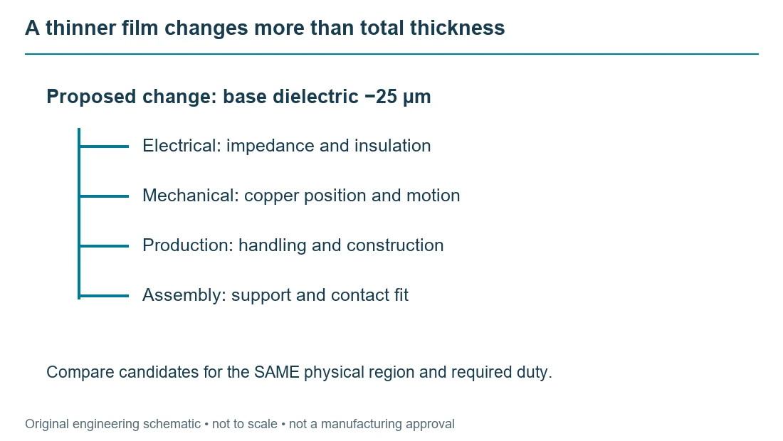
Assume a design team needs more motion clearance. The first proposal is to reduce the base dielectric by 25 µm. Before accepting it, list the dependencies: impedance, insulation, handling, coverlay registration and the supplier's available construction. Compare this proposal with reducing finished copper where electrical loading allows, moving a support edge away from the bend, or changing the enclosure route. Each alternative changes a different part of the design and needs a different verification method.
Record two candidates in separate exports with the same region name and units. Compare their total thickness and copper positions, then ask the fabricator to review realistic finished dimensions. Keep the required bend radius and motion history outside the arithmetic conclusion. A smaller total may help packaging while still leaving a conductor too far from the effective neutral axis, a via in the moving area or an unacceptable local stress concentration.
When comparing quotations, send the same released construction to both suppliers. If one quote assumes an adhesive-based core and another an adhesiveless laminate, a price difference is not necessarily an efficiency difference. Request an explicit exception list. The flex PCB cost worksheet separates panel, recurring and setup assumptions, allowing you to compare costs after the engineering scope is made equivalent.
Flex stackup questions
Does two-layer flex mean two physical sheets?
No. It normally describes the number of conductive copper layers. Film, adhesive, protection and local support introduce additional physical constituents. State their order and extent rather than relying on the copper count to communicate the complete construction.
Can the worksheet recommend a minimum bend radius?
It calculates a thickness proposal only. Bend design depends on the actual construction, conductor position, loading and motion history. Use the design-guideline page to document those conditions, then agree a verification plan. No universal radius multiplier in this worksheet guarantees fatigue life.
Is a multilayer stack always symmetric?
No. The required electrical and mechanical structure may be asymmetric, but that choice should be intentional. Symmetry in nominal material thickness is not proof of balanced copper coverage, uniform adhesive flow or acceptable deformation. Review the finished regional construction, not only the list of purchased films.
What should I send for a stackup review?
Send the circuit revision, copper-layer mapping, constituent list, finished thickness requirements by region, coverlay and stiffener drawings, motion conditions, impedance requirements if applicable and quantities. Mark unresolved items rather than guessing an exact material grade. The worksheet export is supporting information, not a replacement for fabrication data.
Product details for your design review
Existing RAYPCB gallery images illustrate circuit form. Ask for construction-specific records to establish layer count, material, tolerances and test results.
Questions to resolve before ordering
Why does the worksheet sum allowances instead of showing yield?
It calculates a worst-case arithmetic interval from your entries. Statistical distributions, process correlation and finished-thickness measurements are not available to this model.
Can I compare different regions in A and B?
You can retain them as records, but they are not interchangeable candidates. For an alternative-construction decision, compare the same region and requirements.
From a preliminary question to a build-ready enquiry
| Your project stage | Send what you already have | Define before release |
|---|---|---|
| Concept / budget | Application, sketch or approximate outline, installation/motion conditions and quantity range. Unknowns are welcome. | Candidate construction, unresolved dimensions, cost assumptions and whether assembly is included. |
| Design ready | Artwork, drill data, drawing/revision and requested quantity. Identify critical contacts, bend zones and inspection requirements. | Approved stackup, controlled revision, finish, tooling and inspection scope; confirm the lead-time starting conditions. |
| Assembly / transfer | BOM, placement and assembly information where available; supply responsibility, existing test baseline and known issues. | Permanent supports versus temporary carriers, first-article acceptance, test ownership, delivered shape and packaging. |
Compare the full quotation scope
Separate recurring manufacture from one-time tooling, carriers and test development. Compare the same material definition, finish, delivered state and acceptance evidence. A low unit price can exclude a carrier or inspection record required by your product. Request lead time against the actual materials, released files and agreed work; a target date is not a delivery guarantee.
Make sample approval useful for the next batch
Identify the drawing revision and acceptance criteria used for the first build. Record approved material substitutions and resolved engineering questions rather than relying on an email label such as “same as last time.” Ask which dimensional, electrical and construction records are included, which require separate development, and how changes will be approved before a repeat order.
Send your existing files directly, or generate a brief above and choose Carry Brief to Enquiry. Review the message and attach the actual files on Contact before submitting.
Deliver a stackup that another engineer can reproduce

The final stackup table should list region, layer order, function, material designation, copper construction, nominal thickness, bounds and the source of those bounds. Add impedance requirements and mechanical limits as separate constraints. Include the revision of the connector drawing or enclosure model that fixes a local dimension. This creates a reproducible record even when one supplier later changes a product code or suggests an alternative.
A useful release check is to give the table and flat drawing to another engineer and ask them to sketch three sections: free span, contact area and supported component area. If they must guess which layers disappear, the package needs clarification. Reconcile the table with the actual manufacturing outputs, not only the CAD editor. A PDF annotation that never reaches the released artwork can leave the design intent disconnected from the build files.
Use the worksheet to prepare questions for PCB manufacturing review. Include prototype and later production quantities, because material selection and panel planning may need to support both. Do not treat a proposed stackup as stock confirmation or a delivery guarantee. Request explicit agreement on the construction, tolerances and inspection scope for the order. When samples are received, store the measured results against the approved revision and note which product tests used them. This record makes future changes easier to evaluate: a connector change, copper change or coverlay substitution can be traced to the affected region rather than forcing a complete redesign discussion. The value of the stackup is its ability to coordinate decisions, not the number of decimal places or the visual complexity of its drawing.
