Contact Sales & After-Sales Service

Contact & Quotation

  • Inquire: Call 0086-755-23203480, or reach out via the form below/your sales contact to discuss our design, manufacturing, and assembly capabilities.
  • Quote: Email your PCB files to [email protected] (Preferred for large files) or submit online. We will contact you promptly. Please ensure your email is correct.
Drag & Drop Files, Choose Files to Upload You can upload up to 3 files.

Notes:
For PCB fabrication, we require PCB design file in Gerber RS-274X format (most preferred), *.PCB/DDB (Protel, inform your program version) format or *.BRD (Eagle) format. For PCB assembly, we require PCB design file in above mentioned format, drilling file and BOM. Click to download BOM template To avoid file missing, please include all files into one folder and compress it into .zip or .rar format.

PCBSync · PCB surface finish engineering

ENIG PCB: Immersion Gold Finish for Your Assembly

Plan an electroless nickel immersion gold PCB around the pad geometry, connection process and evidence your build needs. Review the nickel and gold layers separately and send PCBSync a clear fabrication request.

Prototype through production · scope and schedule confirmed after file review

Green bare circuit board with a dense pad array and plated hole locations.
At a glance: ENIG combines an electroless nickel layer with thin immersion gold. Gold protects the underlying surface before soldering; it is not a substitute for selective hard gold on a repeated-wear contact.
Prepare a clearer project request

ENIG PCB tools

ENIG PCB workbench

PCBSync Engineering Tools · no account required · calculations run in your browser

Mark what you have prepared

Match the scope to the decision

ENIG PCB: scope, limitations and evidence

Decision / stageWhat to defineEvidence or next action
ConnectionSoldering, bonding or mating functionMap regions that require different review
Nickel layerSpecified requirement and measurement basisLayer-specific lot record
Gold layerSpecified requirement, unit and samplingNo inferred acceptance from color
Process qualityApplicable corrosion and solderability criteriaRequested evidence and disposition route
Assembly handoffPackaging, heat cycles and opening historyConfirmed handling instructions
Practical engineering and purchasing guidance

Specify the finish for the actual connection

Understand what each layer contributes

Electroless nickel forms the barrier between copper and the outer gold layer. Immersion gold protects that surface until assembly and normally dissolves into the solder during joining. The resulting connection must be evaluated as a solder system, not simply as a gold-colored pad.

The planar deposit makes ENIG a candidate for dense surface-mount layouts, but finish selection cannot correct a poor land pattern, filled-via requirement or an unsuitable solder-paste stencil. Send the smallest package geometry and any via-in-pad details for a combined fabrication review and BGA assembly review where array packages are involved.

Specify thickness without losing the measurement basis

Call out the required finish specification and revision, layer requirements and measurement locations. Nickel and gold readings are separate quantities. A supplier report should identify the actual lot, instrument method, calibration basis and sampling arrangement so a number can be interpreted correctly.

Use the workbench to convert micrometers and microinches for three readings of one layer. One microinch equals 0.0254 micrometers. A converted average is not proof that every location meets a limit, and the tool does not assess uncertainty or replace the contractual acceptance method.

Treat corrosion quality as its own question

ENIG process control includes the condition of the nickel deposit and its interaction with the gold deposition process. Excessive nickel corrosion, often discussed as black pad, cannot be ruled out by a visually bright gold surface or by a single thickness value.

Request the process-quality evidence required by the applicable specification and your project. If an assembly failure occurs, preserve lot identity, samples and the thermal history for investigation. Avoid declaring every dark pad a black-pad defect or promising that a particular thickness alone eliminates the mechanism.

Qualify special connections before approving the finish

Repeated mating, wire bonding and sensitive RF paths add requirements beyond ordinary solder lands. Hard gold may be relevant to wear contacts; ENEPIG or other qualified finishes may be considered for bonding. For high-frequency PCB manufacturing, nickel-containing finishes should be assessed against the actual RF structure rather than a general frequency threshold.

PCBSync can review the intended connection map, quantity and assembly route. Ask the quotation to identify the agreed finish, exceptions, storage instructions and requested lot records. Keep substitutions subject to the appropriate engineering approval and link the final choice to the released drawing.

Keep the review concrete

Include these requirements in your enquiry

01

Controlled fabrication drawing and ENIG specification revision.

02

Pad geometry, smallest package and via-in-pad details.

03

Separate nickel and gold requirements with units.

04

Requested sampling, measurement and corrosion-quality records.

05

Assembly route, storage conditions and planned use.

06

Quantity, delivery requirement and approval owner for exceptions.

Mark unresolved items explicitly. Ask the quotation to identify proposed exceptions, required customer approvals and any inspection or special-process charges that remain open.

See the physical construction

Real boards: pads, contacts and assembly context

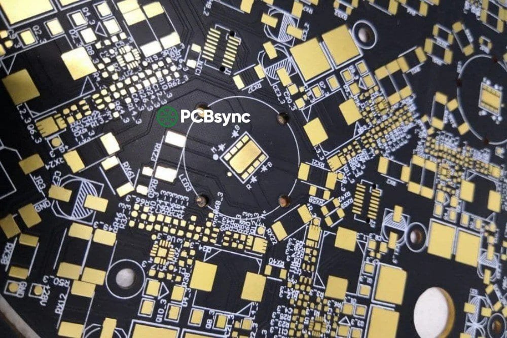
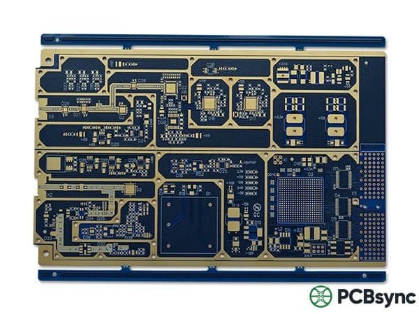
These real photographs from the PCBSync media library show physical board construction and connection features. Appearance alone does not verify finish chemistry, coating thickness or lot acceptance; request the corresponding manufacturing records.

Browse the supporting pages

ENIG PCB guide library

2 supporting guides

Answers before requesting a quote

ENIG PCB FAQ

What does ENIG stand for?

Electroless Nickel Immersion Gold: a nickel barrier with a thin immersion-gold outer finish over the exposed copper features.

Does a gold thickness report prevent black pad?

No. Process condition and the specified corrosion assessment matter separately. Thickness alone cannot establish the absence of nickel corrosion.

Is ENIG suitable for all wire bonding?

No. Wire material, bonding process and acceptance evidence must be qualified together. Discuss ENEPIG or other finishes where appropriate.

How much does an ENIG PCB cost?

Pricing depends on the board, panel, quantity, finish scope and inspection requirements. Send controlled files for a reviewed quote rather than relying on a universal surcharge.

Technical links checked 3 October 2026. Apply the current documentation and project-specific acceptance requirements. Planners do not certify manufacturability or validate uploaded design files.

From planning to a reviewed quotation

Discuss your ENIG PCB requirements

Send the scope you want reviewed

Add your finish-selection brief or planning scenario from the tools above. Include the controlled product revision, requested quantity, required timing and open acceptance questions.

Prepare the fabrication drawing, Gerber or ODB++ data, quantity and delivery requirement. Identify the specified finish, exposed pad locations, assembly route and requested inspection records. Ask us about an NDA or file-transfer arrangement before sharing restricted files.

Email: [email protected]
Phone: +86-755-23203480

Review the message and attachments before sending. An enquiry does not place an order.

Drag & Drop Files, Choose Files to Upload You can upload up to 3 files.