Contact Sales & After-Sales Service

Contact & Quotation

  • Inquire: Call 0086-755-23203480, or reach out via the form below/your sales contact to discuss our design, manufacturing, and assembly capabilities.
  • Quote: Email your PCB files to [email protected] (Preferred for large files) or submit online. We will contact you promptly. Please ensure your email is correct.
Drag & Drop Files, Choose Files to Upload You can upload up to 3 files.

Notes:
For PCB fabrication, we require PCB design file in Gerber RS-274X format (most preferred), *.PCB/DDB (Protel, inform your program version) format or *.BRD (Eagle) format. For PCB assembly, we require PCB design file in above mentioned format, drilling file and BOM. Click to download BOM template To avoid file missing, please include all files into one folder and compress it into .zip or .rar format.

PCBSync · PCB surface finish engineering

OSP PCB: Surface Finish, Assembly Window & Quote

Choose an OSP PCB with an assembly plan as clear as the fabrication drawing. Review pad geometry, thermal passes, handling and the agreed storage window before releasing an order.

Prototype through production · scope and schedule confirmed after file review

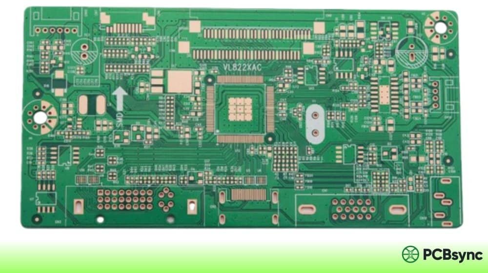
Green bare circuit board with copper-colored exposed pad areas.
At a glance: Organic solderability preservative protects exposed copper with a thin organic coating before soldering. It is not a metal plating and should not be treated as a wear-contact finish.
Prepare a clearer project request

OSP PCB tools

OSP PCB workbench

PCBSync Engineering Tools · no account required · calculations run in your browser

Mark what you have prepared

Match the scope to the decision

OSP PCB: scope, limitations and evidence

Decision / stageWhat to defineEvidence or next action
CoatingOrganic protection over copperApproved OSP process
AssemblyThermal passes, flux and reworkQualified process route
TimingElapsed time plus planned delayAgreed limit and start event
HandlingPackaging, opening and pad contactLot-level exposure record
EvidenceSolderability and traceability needsAgreed inspection package
Practical engineering and purchasing guidance

Specify the finish for the actual connection

Match OSP to the assembly route

OSP can provide a planar solderable surface without adding a nickel barrier or precious-metal layer. Its suitability depends on the actual coating process and the soldering route. Describe single- or double-sided PCB assembly, through-hole operations and any expected rework.

Do not impose one universal number of allowed reflow cycles. Commercial OSP processes differ, and suppliers publish process-specific thermal capabilities. Ask for the offered chemistry and a route qualified for your board rather than assuming every OSP system behaves identically.

Plan the fabrication-to-assembly interval

Agree the storage limit, start event, packaging and exposure conditions in writing. Record shipment and planned assembly dates alongside lot identity. A limit for unopened packaging is not automatically an allowed exposure time after the bag is opened.

The schedule tool compares elapsed time and planned delay with your own agreed limit. It shows margin, not remaining solderability. If conditions changed, records are missing or the calculated window is exceeded, request an engineering disposition rather than simply changing the limit to make the display positive.

Protect exposed pads and test access

Handle boards by suitable edges and keep pad contamination under control. Plan printing, cleaning and probing with the assembler; test-pad contact needs review because an organic coating is present. Copper appearance alone cannot establish coating condition or acceptance.

Specify any contact areas that need a different qualified finish. Repeated sliding connectors and bonding interfaces are distinct requirements from a solder land. Mark those regions on the drawing instead of asking one finish to perform incompatible tasks without review.

Build an RFQ that includes handling

Send the fabrication files, quantities, assembly sequence and intended inventory policy. Identify whether PCBSync supplies bare boards or coordinates assembly as well. Ask the quotation to state finish scope, packaging, schedule assumptions and requested evidence.

For repeat manufacturing, track lot dates and revised assembly plans. Split deliveries may be worth comparing when inventory would otherwise sit for a long period. Any storage extension, reprocessing or solderability evaluation needs approval against the actual board and process history.

Keep the review concrete

Include these requirements in your enquiry

01

Controlled files and OSP finish requirement.

02

Reflow, through-hole and planned rework sequence.

03

Agreed storage limit with its start event and conditions.

04

Packaging and opened-bag handling requirements.

05

Probe pads, contact interfaces and any finish exceptions.

06

Lot quantities, delivery schedule and requested records.

Mark unresolved items explicitly. Ask the quotation to identify proposed exceptions, required customer approvals and any inspection or special-process charges that remain open.

See the physical construction

Real boards: pads, contacts and assembly context

These real photographs from the PCBSync media library show physical board construction and connection features. Appearance alone does not verify finish chemistry, coating thickness or lot acceptance; request the corresponding manufacturing records.

Browse the supporting pages

OSP PCB guide library

2 supporting guides

Answers before requesting a quote

OSP PCB FAQ

Can OSP survive more than two reflow passes?

Some specific processes support multiple passes. There is no universal count for every OSP chemistry and assembly route; qualify the offered process.

Does OSP protect a finished product for its entire service life?

Its primary role is protecting copper before soldering. Finished-product environmental protection and reliability need separate design and validation.

Does the schedule tool approve old stock?

No. It calculates a time margin from your inputs. Condition history and required solderability evidence still control release.

Technical links checked 3 October 2026. Apply the current documentation and project-specific acceptance requirements. Planners do not certify manufacturability or validate uploaded design files.

From planning to a reviewed quotation

Discuss your OSP PCB requirements

Send the scope you want reviewed

Add your finish-selection brief or planning scenario from the tools above. Include the controlled product revision, requested quantity, required timing and open acceptance questions.

Prepare the fabrication drawing, Gerber or ODB++ data, quantity and delivery requirement. Identify the specified finish, exposed pad locations, assembly route and requested inspection records. Ask us about an NDA or file-transfer arrangement before sharing restricted files.

Email: [email protected]
Phone: +86-755-23203480

Review the message and attachments before sending. An enquiry does not place an order.

Drag & Drop Files, Choose Files to Upload You can upload up to 3 files.