Contact Sales & After-Sales Service

Contact & Quotation

  • Inquire: Call 0086-755-23203480, or reach out via the form below/your sales contact to discuss our design, manufacturing, and assembly capabilities.
  • Quote: Email your PCB files to [email protected] (Preferred for large files) or submit online. We will contact you promptly. Please ensure your email is correct.
Drag & Drop Files, Choose Files to Upload You can upload up to 3 files.

Notes:
For PCB fabrication, we require PCB design file in Gerber RS-274X format (most preferred), *.PCB/DDB (Protel, inform your program version) format or *.BRD (Eagle) format. For PCB assembly, we require PCB design file in above mentioned format, drilling file and BOM. Click to download BOM template To avoid file missing, please include all files into one folder and compress it into .zip or .rar format.

PCB design · Layout · Production handoff

PCB Design Services

PCB layout and design review, with manufacturing in mind.

Need a new PCB layout, a board revision or a design review? Bring your schematic, constraints and open questions to PCBSync. Define the work, review points and release files before the project starts.

Already have production files? PCB fabrication · PCB assembly

PCB layout in CAD software showing component placement and copper routing.
PCB LAYOUT & ROUTING Component placement and copper routing in a PCB design workspace.

PCB design turns a circuit schematic and product constraints into component placement, copper routing, a layer stack-up and fabrication data. A PCB design service adds an agreed engineering scope, review process and deliverable package. PCB layout, circuit development and production testing are separate tasks; specify which you need.

A useful place to start

Build a better design brief.

Choose your starting point. Get a tailored input checklist and cost drivers, then add the brief to your inquiry. No account needed.

Requested format; compatibility is confirmed in the quote.

Include in the scope discussion
Prepare the layout inputs

Schematic and BOM, board outline, connector positions, footprints and routing constraints.

Explore the stack-up builder →

Your project outline

Ready for a useful conversation.

The planner runs in your browser. Nothing is sent until you submit the inquiry.

Start at the right stage

What do you need designed?

01 / NEW LAYOUT

A schematic ready for a board.

Share the circuit, bill of materials, mechanical envelope and interface requirements. Define placement priorities, stack-up, routing rules and the review checkpoints for the layout.

Important input: approved component footprints and connector locations.

02 / BOARD REVISION

Change the board with control.

Identify the released revision, the requested changes and everything that must stay compatible. Include known faults, component replacements and test evidence where available.

Important input: a change list linked to the existing design revision.

03 / DESIGN REVIEW

Resolve manufacturing questions.

Review fabrication and assembly constraints before release: spacing, hole structures, solder mask, component access and the completeness of the output package.

Important distinction: DFM review does not verify circuit function.

04 / EARLY CONCEPT

Make the scope explicit first.

If you have requirements rather than a schematic, describe the functions, interfaces, power, size and environment. Circuit development, firmware, simulation and enclosure work need separate scope confirmation.

Important input: acceptance criteria, assumptions and unresolved decisions.

Agree the outputs before starting

Buy a usable release package.

Specify the files your next engineer and your manufacturer will need. The final quotation identifies the included outputs, formats and review responsibilities.

PCB design handoff checklist
PackageWhat to agreeWhy it matters
Editable designCAD application/version, source schematic and layout where included, symbols, footprints, linked libraries and ownership terms.Lets your team maintain the next revision. Gerbers alone are not an editable CAD project.
PCB fabricationGerbers or an agreed intelligent data format, drill files, outline, layer map, stack-up and fabrication drawing.Communicates copper, holes, materials, finish and tolerances without conflicting revisions.
PCB assemblyBOM with manufacturer part numbers and DNP items, placement coordinates, assembly drawings, polarity and special-process notes.Keeps purchasing, stencil preparation and placement aligned.
Review & releaseDRC/ERC findings as applicable, approved exceptions, revision history and documented customer sign-off.Makes the release decision traceable; a passed rule check is not a functional test.

Need help preparing an existing package? See PCB file formats and design for manufacturing.

Review each stage with the right checklist: schematic review, layout review and the complete design release review.

  1. Agree the brief

    Requirements, inputs, responsibilities, price, milestones and change policy.

  2. Review placement

    Mechanical fit, connectors, critical components and proposed stack-up.

  3. Review routing

    Constraint checks, reference paths, fabrication limits and open exceptions.

  4. Release & validate

    Approve one file revision; define the prototype assembly build, bring-up and tests.

Decisions that improve the board

Design tips before routing starts.

Use the right constraints early. A calculator is a starting point; approve the physical stack-up, material and test conditions with the manufacturer.

1. Define the stack-up first

For a multilayer PCB, reserve signal and reference layers, agree dielectric thicknesses and copper, and check the fabrication route before committing to controlled-impedance geometry.

Stack-up builder →

2. Design the return path

Check where high-frequency return current will flow, including layer transitions. Avoid routing critical signals across breaks in their reference plane. Edge rate matters, not only clock frequency.

High-speed design guide →

3. Calculate power with context

Size conductors against current, allowed temperature rise, copper thickness, layer position and voltage drop. Thermal behavior also depends on the surrounding board and enclosure.

Trace-width calculator →

4. Leave room to build & test

Check actual package drawings, polarity, assembly clearances and access to test points. Define probing, programming and fixture needs before the layout is frozen.

Test-access considerations →

From screen to physical board

Design choices have manufacturing consequences.

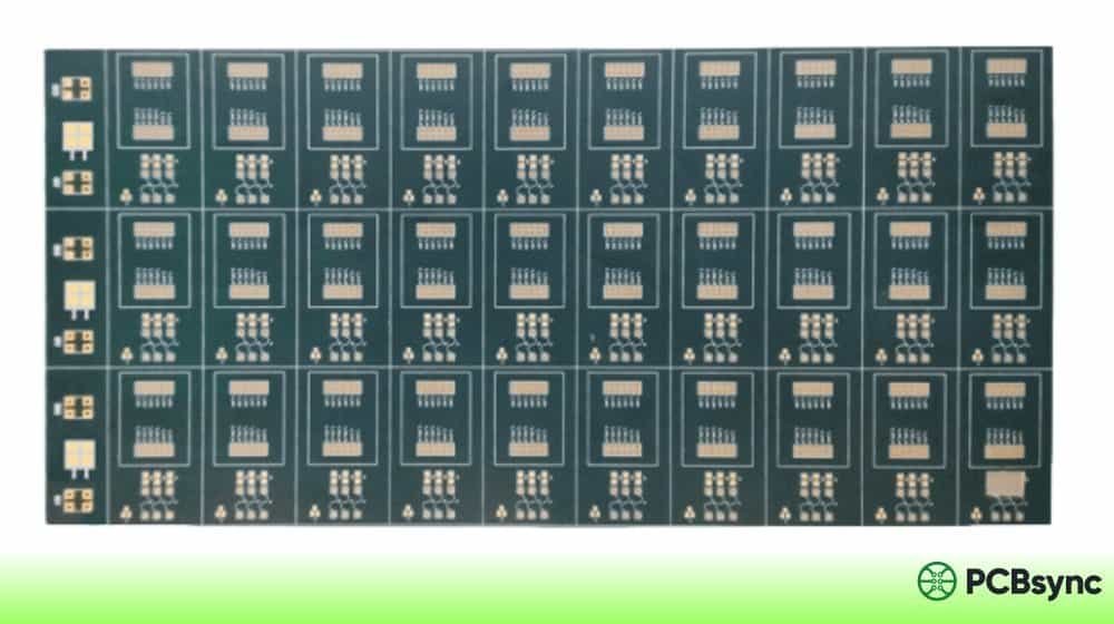
Fabricated green PCB panel with repeated pad patterns and routing features.

Fabrication details

Pad geometry, clearances, via structure and panel constraints belong in the design review.

Plan PCB fabrication →
SMT placement equipment on a PCB assembly line.

Assembly access

Placement, component orientation and process clearances affect the assembly route.

Plan PCB assembly →
Populated circuit board positioned in an inspection and test fixture.

Test access

Probe access and fixture clearance need to be considered before the production release.

Review quality & test evidence →

Physical boards, equipment and a test fixture from the PCBSync media library. These images illustrate manufacturing considerations; they are not attributed design case studies.

Price & schedule

What affects a PCB design quote?

Board area and layer count are only part of the workload. A small RF board or a dense BGA escape can require more engineering than a larger, simpler layout.

  • Input quality: schematic completeness, usable libraries and fixed mechanical constraints.
  • Routing difficulty: pin density, interfaces, impedance, length matching and via structure.
  • Review scope: analysis, documentation, revision rounds and prototype support.
  • Release needs: native file format, output package and acceptance criteria.

Ask for design fees, prototype fabrication, components, assembly and test to be separated. Lead time should state which inputs and approvals start each milestone.

Questions before you hire

PCB design service FAQs

Clear boundaries help purchasing and engineering make the same decision.

What should I send for a PCB layout quotation?

Send the schematic, BOM, board outline, connector positions and relevant component data. Include target layers or stack-up, power and signal constraints, required source format, deliverables and target dates. Mark missing information rather than guessing it. A short initial brief is enough to start the scope discussion.

Can I request Altium or KiCad source files?

State the required CAD application and version in the brief. File compatibility, source deliverables, libraries and ownership must be confirmed in the quotation. An image, PDF or Gerber export does not substitute for a maintainable native CAD project.

Does PCB design include a schematic, firmware and enclosure?

Not automatically. Layout normally starts from a defined circuit and constraints. Circuit development, firmware, mechanical design, simulation, compliance work and prototype bring-up are separate scope items. List the work you need so responsibilities and exclusions can be agreed.

Will a DRC pass guarantee the board works?

No. DRC checks the rules and connectivity represented in the CAD project. Incomplete rules, an incorrect circuit or an unsuitable component can remain undetected. DFM, assembly review and prototype functional validation address different risks.

Can PCBSync manufacture and assemble the design?

PCB fabrication and assembly can be quoted alongside the design request. Confirm the construction, sourcing responsibility, acceptance criteria, test scope and approved revision before release. Read the quality-control page for the reports and checks to discuss with your purchasing team.

How should confidential designs and revisions be handled?

Request the NDA process before sharing restricted files. Agree the source-file ownership, permitted access and revision-control process in writing. Define which customer approvals release placement, routing and production data, and how changes after approval are priced.

Your next board

Tell us where you need help.

Describe the board, current design stage and the output you need. Add the target date and unresolved questions. Files are optional for the first conversation.

What happens next: the request is reviewed to clarify inputs, feasibility, deliverables and quotation scope. Design work and production release require an agreed project scope.

[email protected]
+86 755 2320 3480

You can type directly into the form; the brief planner is optional. Need an NDA first? Say so in your message.

Drag & Drop Files, Choose Files to Upload You can upload up to 3 files.

Working on the design yourself?

Start with the online PCB design workflow, then continue with the guide to choosing PCB design services, controlled-impedance requirements or PCB antenna design considerations.

Technical references: KiCad PCB Editor documentation · Altium PCB design documentation. Reference links explain design workflows; they do not imply an affiliation or a confirmed software deliverable.