Contact Sales & After-Sales Service

Contact & Quotation

  • Inquire: Call 0086-755-23203480, or reach out via the form below/your sales contact to discuss our design, manufacturing, and assembly capabilities.
  • Quote: Email your PCB files to [email protected] (Preferred for large files) or submit online. We will contact you promptly. Please ensure your email is correct.
Drag & Drop Files, Choose Files to Upload You can upload up to 3 files.

Notes:
For PCB fabrication, we require PCB design file in Gerber RS-274X format (most preferred), *.PCB/DDB (Protel, inform your program version) format or *.BRD (Eagle) format. For PCB assembly, we require PCB design file in above mentioned format, drilling file and BOM. Click to download BOM template To avoid file missing, please include all files into one folder and compress it into .zip or .rar format.

PCBSync · Inspection, test & quality planning

PCB Test Points: Design Access for Fabrication, Assembly and Debug

Choose testpoint locations around the measurements your board needs. Separate bare-board access, assembled-board contact and engineering debug so each output serves its intended user.

Prototype through production · scope and schedule confirmed after file review

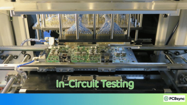
Close view of test probes contacting a populated circuit board.
At a glance: A testpoint is a physical access location, not a test result. Its usefulness depends on net selection, assembled clearance, measurement behavior and the method that contacts it.
Prepare a clearer project request

PCB Test Points tools

PCB Test Points workbench

PCBSync Engineering Tools · no account required · calculations run in your browser

Mark what you have prepared

Match the scope to the decision

PCB Test Points: scope, limitations and evidence

Decision / stageWhat to defineEvidence or next action
PurposeFabrication, assembly or debugAttributed access list
LocationNet, coordinate, side and originConsistent CAD output
GeometryPad, mask, finish and clearanceProvider-specific contact rules
Signal integrityLoading, return path and sensitive nodesElectrical review
ReleaseVariants, ECOs and exclusionsControlled report and review
Practical engineering and purchasing guidance

Define the test before approving the result

Assign a purpose to each access location

Fabrication testing concerns the unpopulated board. Assembly testing must account for fitted components and the chosen test method. Engineering debug may need an operator-accessible connector, pad or fitted testpoint with a suitable reference connection. These purposes can share a location, but they should not be assumed equivalent.

Maintain separate or clearly attributed output lists for each use. In CAD tools that distinguish fabrication and assembly testpoints, configure the appropriate rules and assignments. The delivered report should identify net, coordinate, side and revision in the agreed format.

Agree contact geometry with the test provider

Pad size, spacing, mask opening, finish and surrounding height affect access. The acceptable geometry depends on the probe, fixture, manufacturing variation and assembled product. Obtain the actual contact requirements before setting design rules; a value copied from an unrelated project is not a universal standard.

Review access on both sides and after any shielding, coating or enclosure work. Allow for location tolerances, support and collision clearance. Mark surfaces that must remain untouched and identify alternatives where the test method cannot contact a required node reliably.

Protect the measurement you are trying to make

An added pad, stub or long probing connection can disturb a sensitive signal. Low-resistance measurement can also be dominated by lead and contact resistance. Review access with the circuit designer and test engineer instead of adding a pad to every net without considering electrical consequences.

The lead-resistance tool illustrates a simple two-wire series contribution using entered milliohm values. It does not model probe inductance, high-frequency behavior, instrument uncertainty or a complete Kelvin measurement. Use the result to identify a discussion point, not to approve a measurement setup.

Verify exports against the assembled design

Before release, run the applicable design checks and review the testpoint report against the intended board side, origin and net naming. Confirm that optional components and mechanical parts do not block the locations needed for each product variant.

Provide PCBSync with the layout, report and desired test methods early enough to resolve access gaps. Record agreed exceptions and the alternative checks for affected requirements. After an ECO, regenerate the outputs and have the changed access reviewed with the program or fixture owner.

Keep the review concrete

Include these requirements in your enquiry

01

Required measurements and critical nets

02

Separate fabrication/assembly/debug purposes

03

Agreed contact geometry and clearances

04

Coordinate origin, units and board side

05

Assembled geometry and variant review

06

Testpoint output and documented exceptions

Mark unresolved items explicitly. Ask the quotation to identify proposed exceptions, required customer approvals and any inspection or special-process charges that remain open.

See the physical construction

Test contacts, equipment and real PCB assemblies

These real photographs show physical contact and assembled-board geometry. Use them as inspection context; the quotation should identify the actual fixture, instrument configuration and validated program for your product.

Answers before requesting a quote

PCB Test Points FAQ

Can an exposed via be a testpoint?

It may be suitable if its geometry, finish, access and intended measurement meet the reviewed requirements. Exposure alone is not enough.

What is the correct universal testpad size?

There is no single value for every probe, fixture and board. Agree the geometry and tolerances for the selected method.

Does a testpoint report prove coverage?

It documents assigned access. The program must still implement and validate meaningful checks for the requirements.

Technical links checked 3 October 2026. Apply the current documentation and project-specific acceptance requirements. Planners do not certify manufacturability or validate uploaded design files.

From planning to a reviewed quotation

Discuss your PCB Test Points requirements

Send the scope you want reviewed

Add your test-scope brief or planning scenario from the tools above. Include the controlled product revision, requested quantity, required timing and open acceptance questions.

Share the controlled schematic, BOM/options, intelligent layout or netlist data, testpoint report and assembled mechanical information. Include the intended test platform or existing fixture/program, target measurements, acceptance requirements, quantity/forecast and report needs. Identify missing inputs and any access restrictions.

Email: [email protected]
Phone: +86-755-23203480

Review the message and attachments before sending. An enquiry does not place an order.

Drag & Drop Files, Choose Files to Upload You can upload up to 3 files.