Contact Sales & After-Sales Service

Contact & Quotation

  • Inquire: Call 0086-755-23203480, or reach out via the form below/your sales contact to discuss our design, manufacturing, and assembly capabilities.
  • Quote: Email your PCB files to [email protected] (Preferred for large files) or submit online. We will contact you promptly. Please ensure your email is correct.
Drag & Drop Files, Choose Files to Upload You can upload up to 3 files.

Notes:
For PCB fabrication, we require PCB design file in Gerber RS-274X format (most preferred), *.PCB/DDB (Protel, inform your program version) format or *.BRD (Eagle) format. For PCB assembly, we require PCB design file in above mentioned format, drilling file and BOM. Click to download BOM template To avoid file missing, please include all files into one folder and compress it into .zip or .rar format.

PCB Manufacturing / Glass PCB
PCBSync · PCB materials & manufacturing

Glass PCB: Define the Optical Area and Circuit Structure

Plan a glass PCB with the right substrate, conductor pattern and assembly constraints. Explore optical-layout open area, distinguish rigid glass circuits from transparent flex, and prepare a focused manufacturing review.

Prototype through production · scope and schedule confirmed after file review

Transparent circuit board with copper traces, contact pads and an attached connector.
At a glance: A glass PCB carries an electrical circuit on a glass substrate. It is different from woven-glass epoxy FR-4, and a transparent flexible circuit may use polymer film rather than glass.
Prepare a clearer project request

Glass PCB tools

Glass PCB workbench

PCBSync Engineering Tools · no account required · calculations run in your browser

Mark what you have prepared

Match the scope to the decision

Glass PCB: scope, limitations and evidence

Decision / stageWhat to defineEvidence or next action
Rigid glass circuitGlass chemistry, thickness, conductor and outlineConfirm material and process feasibility for the drawing.
Transparent flexible circuitFilm, adhesive, cover layer and bend requirementUse the transparent PCB guide; do not label film as glass.
Optical zoneWavelength, clear region, viewing direction and cosmetic criteriaEvaluate the assembled optical path, not only bare-sheet clarity.
TGV / double-sided connectionHole function, size and conductive interfaceRequest construction-specific evidence and limits.
Assembly and mountingThermal cycle, support, connections and packagingAgree inspection and handling for the finished deliverable.
Practical engineering and purchasing guidance

Design the process around the real requirement

Choose the function before the glass grade

A glass circuit may be selected for a viewing window, dimensional behavior, an optical interface or an electronic packaging requirement. Those functions do not lead to the same glass specification. Identify the operating wavelength, temperature range, assembly process and mechanical envelope before choosing a chemistry or thickness. A visible-light demonstration does not characterize infrared or ultraviolet transmission.

Keep rigid transparent boards, semiconductor glass-core substrates and temporary glass carriers separate in the RFQ. The linked SCHOTT and Corning resources describe different roles for glass in packaging. Their wafer, panel and through-glass-via technologies illustrate possible constructions; they are not evidence that every glass-board supplier offers those dimensions or processes.

Design an optical window alongside the copper network

Show the region that must remain visually or optically clear and the allowed obstructions. Copper traces, pads, components, adhesives and printed markings can all interrupt that region. Define viewing direction, acceptable cosmetic defects and the method used to evaluate the finished assembly. The clearest bare substrate can still produce a poor viewing window after routing and assembly.

The open-area tool compares a rectangular envelope with the combined opaque area you enter. It counts geometry only and does not predict transmission, haze, reflections or color. Count overlapping features once. For a sensor window, also check the beam position and tolerance; an acceptable overall clear percentage does not ensure that the one critical optical path remains open.

Specify the conductor and connection route

State the conductor material, thickness, minimum geometry and expected electrical duty. Ordinary metal traces remain visible. If the requirement involves a transparent conductive film or a fine metal mesh, name that construction explicitly and review sheet resistance, contact formation and optical performance together. Do not treat it as a cosmetic option on a standard copper circuit.

Through-glass vias require a defined hole-forming and metallization process. Distinguish a plain opening from a conductive interconnect and identify the connection on each face. Confirm routing registration, adhesion and assembly compatibility for the proposed stack. Fine-pitch package-substrate data cannot be applied automatically to a larger transparent display board.

Control handling, mounting and acceptance

A glass board needs mechanical support appropriate to its thickness, outline and edge condition. Show mounting areas, connector insertion loads and any constrained expansion against the enclosure. Specify the assembly thermal cycle and assess the joints and conductor interface as well as the glass itself. A glass softening temperature does not approve a complete assembly for reflow or service.

Send fabrication artwork, a dimensioned drawing, optical-zone requirements, assembly details and quantities to PCBSync. Request confirmation of the offered material, metallization, inspection scope and packaging. PCB prototyping evaluation should include the actual mounted optical path and electrical function. Record accepted cosmetic standards so production inspection does not depend on an undefined promise of transparency.

Keep the review concrete

Include these requirements in your enquiry

01

Glass grade or the optical / mechanical selection requirement

02

Dimensioned outline, thickness and mounting details

03

Conductor pattern and hole / interconnect functions

04

Critical clear zones and optical acceptance method

05

Assembly process and connector / attachment details

06

Prototype quantity, production forecast and inspection scope

Mark unresolved items explicitly. Ask the quotation to identify proposed exceptions, required customer approvals and any inspection or special-process charges that remain open.

See the physical construction

Real transparent glass-circuit examples

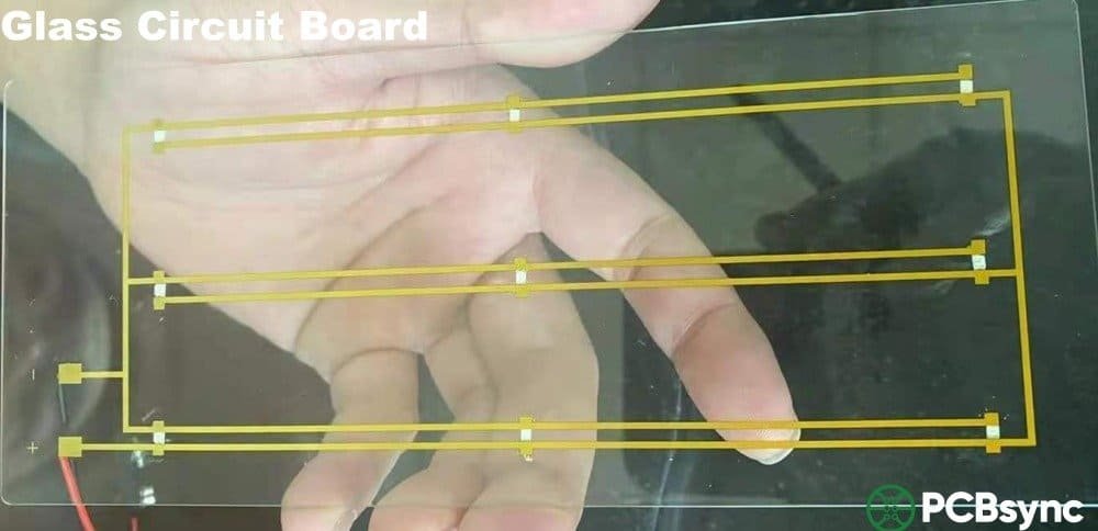
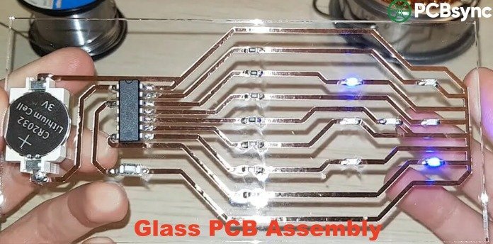
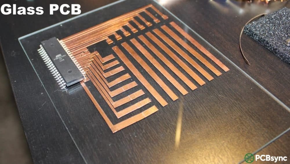
These photographs show visible conductor patterns and a populated transparent assembly. A photograph cannot verify glass chemistry, spectral transmission, TGV geometry or production qualification.

Browse the supporting pages

Glass PCB guide library

1 supporting guides

Answers before requesting a quote

Glass PCB FAQ

Is glass PCB the same as FR-4?

No. FR-4 uses woven glass reinforcement in an epoxy laminate. This page concerns circuits supported by a glass substrate.

Can a glass PCB be flexible?

Some very thin glass constructions can bend under controlled conditions, but bend capability must be specified and qualified. A transparent film circuit is a different material system.

Does PCBSync offer every TGV capability shown by glass suppliers?

Capabilities are confirmed for the exact material, hole, metallization and drawing. Third-party glass-supplier examples are technical context, not PCBSync production specifications.

What files help with a glass PCB quotation?

Provide circuit artwork, dimensions, material or selection requirements, clear zones, assembly process, quantity and acceptance criteria. Identify whether the deliverable is a bare circuit, populated board or packaging substrate.

Technical links checked 3 October 2026. Apply the current documentation and project-specific acceptance requirements. Planners do not certify manufacturability or validate uploaded design files.

From planning to a reviewed quotation

Discuss your Glass PCB requirements

Send the scope you want reviewed

Add your project brief or planning scenario from the tools above. Include the controlled product revision, requested quantity, required timing and open acceptance questions.

Prepare the fabrication drawing, Gerber or ODB++ data, quantity and delivery requirement. Identify copper weights, critical geometry, layer spans, fabrication tolerances and requested inspection records. Ask us about an NDA or file-transfer arrangement before sharing restricted files.

Email: [email protected]
Phone: +86-755-23203480

Review the message and attachments before sending. An enquiry does not place an order.

Drag & Drop Files, Choose Files to Upload You can upload up to 3 files.