UL · ISO 9001
Quality documentation & scope →
Choose the board construction
Multilayer FR-4, HDI, flex, rigid-flex, RF and ceramic fabrication routes.
Compare technologies →
UL · ISO 9001
Quality documentation & scope →
PCBSync / bare-board fabrication
Bare-board fabrication for prototypes and repeat production. Compare board technologies, define your fabrication requirements and request a quotation for the approved design.
Gerber files ready? Request a quote directly. Still planning? Start with the calculator below.

Multilayer FR-4, HDI, flex, rigid-flex, RF and ceramic fabrication routes.
Compare technologies →Review published capability ranges alongside your material, copper, stack-up and via requirements.
View rigid PCB specifications →Bare boards, agreed inspection scope and the records your project needs, tied to the approved revision.
Review quality & records →YOUR PCB. YOUR BUDGET.
Choose your PCB type, enter the essentials and compare quantities. Turn your specification into a quotation request when you are ready.
Skip the budget model. Send your Gerbers, quantity and requirements for a project quotation.
Seven technologies. One clear project brief.
Choose your PCB technology and enter the project requirements.
Dimensions and quantity describe individual boards. Requested panelization is reviewed separately.
Enable JavaScript for interactive planning, or send your specifications for a quotation.
This is a planning scenario using existing PCBSync estimator coefficients, not a current production quotation. Rigid and 3–4 oz heavy-copper estimates use the standard FR-4 area, layer, finish, thickness and copper factors. HDI, flex, rigid-flex, RF and ceramic estimates use the former manufacturing-quote page’s technology-specific area, layer and setup allowances.
The ±20% display spread is an illustrative range, not validated prediction accuracy. Specific grades, stack-ups, copper thicknesses and the additions listed for review need a separate quotation. Quantity factors are interpolated to avoid abrupt price jumps. Requested delivery times do not add a made-up expedite fee or reserve capacity.
The ceramic reference scenario is alumina / DPC-style metallization; DBC, AMB, AlN, Si₃N₄ and different copper thicknesses require engineering pricing. Values in the selector describe requests, not guaranteed manufacturing capabilities.
Valid specifications are kept in this browser tab for up to two hours; each technology keeps its own settings and shares quantity with the assembly planner. This tool does not store contact details or design files and does not inspect Gerber files. Model version: 2026.09.30-v3.
Choose your technology
PCB manufacturing creates the bare circuit board: conductive layers, dielectric materials, vias, surface finish and the final outline. Match the fabrication route to signal integrity, thermal performance, mechanical requirements and production volume.
A starting point for many control, power and digital designs. Confirm layer count, stack-up, copper distribution and finished thickness before layout release.
Multilayer PCB →Discuss microvias, sequential lamination and via-in-pad needs early. The build-up structure determines process complexity and must fit the actual routing constraints.
HDI PCB →Define whether the circuit bends during installation or repeatedly in service. Share the bend geometry, stiffeners, transition regions and mechanical envelope.
Flex PCB · Rigid-flex PCB →Specify the exact laminate family and grade, operating requirements and any mixed-material construction. Material choice and stack-up belong in the same review.
Rogers PCB →Share the substrate, metallization, thermal path and assembly requirements. A ceramic design needs a material-specific process review instead of an FR-4 assumption.
Ceramic PCB →Compare the prototype needs with the intended production route. Keep the released revision and acceptance requirements consistent as order quantities grow.
PCB prototyping →Manufacturing fit
A single maximum layer count or minimum feature size cannot establish whether a board is manufacturable. Material, copper, thickness, via geometry and the requested process interact. Submit the fabrication data to confirm their combination.
| Project requirement | Combination to verify | Prepare for review |
|---|---|---|
| Stack-up & finished thickness | Layer construction, dielectric thicknesses, copper distribution and tolerance. | Fabrication drawing, material grade and desired stack-up. |
| Traces, spacing & impedance | Feature sizes at the selected copper weight; impedance targets and reference planes. | Target impedance, tolerance, trace structure and coupon requirements. |
| Drills & vias | Finished holes, plating, aspect ratio, microvia structure and via filling or capping. | Drill files, finished-hole notes and via requirements. |
| Surface finish & solder mask | Finish compatibility with assembly, mask openings, fine-pitch features and marking. | Finish, mask and legend requirements; relevant acceptance criteria. |
| Outline, slots & panelization | Routing, scoring, plated slots, mechanical tolerance and usable panel configuration. | Dimensioned outline, slot notes and assembly panel constraints. |
Use the linked capability pages as a starting point. Your quotation should identify the agreed material, geometry, tolerances and test scope together. A capability listed for one construction is not an approval for every combination.
Continue with rigid PCB capabilities, HDI capabilities, flex capabilities or rigid-flex capabilities. Confirm project-specific limits during engineering review.
Quality & verification
Inspection and electrical verification should follow the agreed board specification. Define the netlist reference, critical dimensions, impedance requirements and records needed before releasing the order.
Bare-board electrical testing checks circuit continuity and isolation. It does not replace a functional test of an assembled product. For critical structures, discuss which measurements or cross-section evidence are appropriate for the project.
Review PCB electrical testing, the PCB laboratory and the quality control process. Request the applicable certification scope and inspection evidence during supplier qualification.

Evidence to agree before release
Specify which records your project needs and agree their scope before ordering. The sequence below is a documentation guide, not a sample test result or a claim that every record is supplied with every order.
Part number, revision, drawing, material and stack-up
Resolved questions, accepted changes and test requirements
Identification, inspection/test records and shipment documents
Supplier qualification
Review the company profile and relevant production capabilities. Confirm the manufacturing and shipping locations for your project, and share your supplier questionnaire.
About PCBSync · Review capabilities →Request the current certificate scope and the inspection or test records relevant to your build. Agree acceptance criteria, traceability and first-article requirements before release.
Quality control · Laboratory overview →Start with a non-confidential brief if you need an NDA. Identify the controlling revision and who can approve substitutions or engineering changes.
Contact the team →What happens after your inquiry? We review the supplied requirements, clarify open technical and material questions, and prepare the quotation scope. Price, lead time and acceptance requirements are confirmed before you authorize production.
From release to delivery
The manufacturing route depends on the board construction. This simplified sequence shows the decisions to settle and the evidence to agree along the way.
Match Gerber, drill data, outline and drawing to one controlling revision. Resolve conflicts before release.
Confirm: the approved file setReview stack-up, material, copper, vias, finish and panelization together with the acceptance requirements.
Confirm: the manufacturing scopeImaging, etching, lamination and hole processing follow the selected construction and manufacturing sequence.
Review: critical process requirementsMask, markings and surface finish are matched to the approved fabrication and downstream assembly needs.
Review: openings and finishAgree the applicable dimensional, visual and electrical checks. Additional evidence must be specified for the project.
Confirm: test scope and recordsMatch identification and delivery documents to the released revision. Confirm packaging and shipping arrangements.
Confirm: quantity and delivery termsIllustrative process map. Actual steps vary by technology; this is not a production traveler.
A familiar part number does not establish that the material, artwork or inspection requirements are unchanged. Send the approved revision and identify each change.
Cost & delivery planning
Layer count, stack-up, material grade, copper weight and board size influence the manufacturing route. Fine features, sequential lamination, via filling and demanding tolerances can add process steps.
Specify only the requirements your design needs, but do not relax electrical, thermal or reliability requirements simply to lower an estimate. Ask which changes are technically acceptable.
Setup and tooling are spread across the batch. Panel utilization, quantity breaks, inspection requirements and delivery timing can change the quoted cost.
Request comparable quotations for the same revision and specification. Separate fabrication from assembly, special testing, freight and taxes so that comparisons remain meaningful.
Confirm whether the manufacturing schedule begins after file approval, material availability or another agreed milestone. Manufacturing time and shipping time are separate. Confirm the destination, shipping method, taxes and any required documentation in the quotation.
PCB project gallery
Explore Rogers / RF, flex, ceramic, HDI, multilayer and rigid-flex samples from the PCBSync product library. Use the construction closest to your design to start a more focused fabrication discussion.
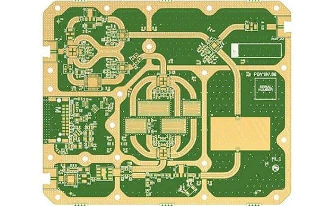
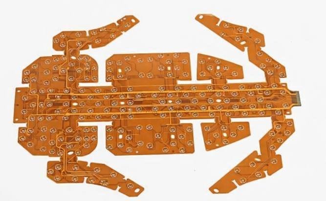

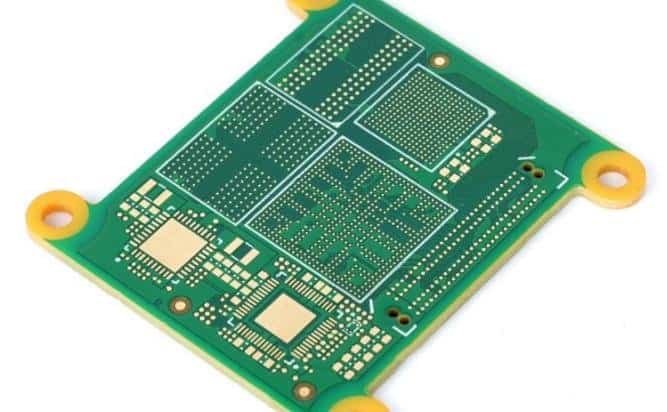
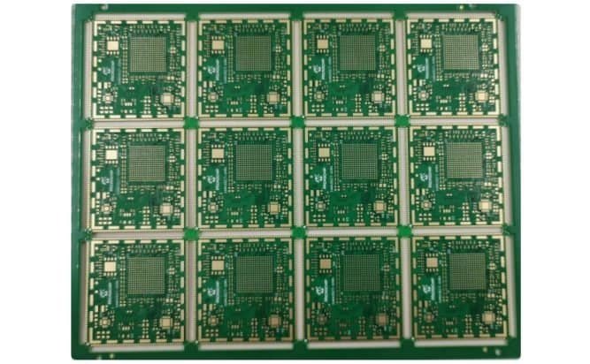
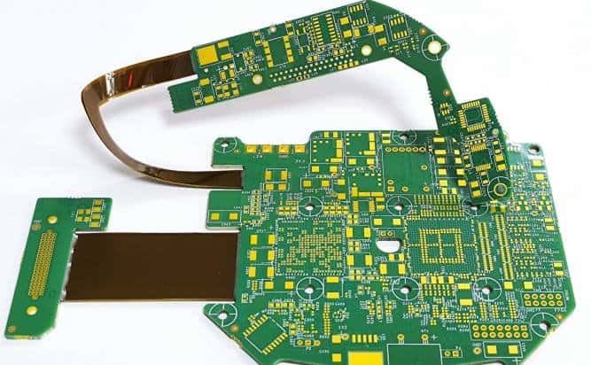
These images illustrate board constructions. Exact materials, layer counts and acceptance criteria are defined by each project’s approved fabrication records.
Design for manufacture
Trace geometry depends on dielectric thickness, material properties and copper. Use the stack-up builder and impedance calculator for early exploration, then review the proposed construction with engineering.
The drill aspect-ratio checker can highlight an early design question. It does not approve a drill process. Distinguish finished holes from drill sizes, specify plated slots clearly, and keep copper clearances consistent with routing and scoring requirements.
For flex and rigid-flex, add bend direction, bend region and installation geometry. For RF designs, name the laminate grade and discuss the impedance control requirements rather than relying on a broad material label.
A practical file guide
Documentation guide. A matching filename alone does not confirm that the data agrees.
Need assembled boards?
Component sourcing, placement, soldering and functional testing are separate from bare-board fabrication. Coordinate panel format, finish, BOM and assembly files for a combined project.
Common fabrication questions
PCB manufacturing produces the bare printed circuit board to the agreed fabrication requirements. Component procurement, placement, soldering and assembled-product testing belong to PCB assembly and can be requested as a combined project.
Provide Gerber and drill data, a fabrication drawing or specification, quantity and delivery requirements. Include the material grade, stack-up, finished thickness, copper, surface finish, impedance targets, special processes and acceptance requirements.
Yes. Choose the matching technology in the calculator. Each option has its own material and construction fields. Requirements outside the reference model are identified for engineering review instead of being silently included in the price.
No. The calculator shows a reference budget from the existing planning model, not a current selling price. Compare scenarios, download your specification and send it through Contact. The reviewed quotation confirms material, process additions, test scope, price and delivery terms.
No. A calculator can help explore a relationship or identify a question, but manufacturing approval depends on the complete combination of geometry, materials, tolerances and process requirements. Submit the design for engineering review.
Use the same controlled revision and explicitly match material, stack-up, finish, tolerances, test scope, quantity and delivery terms. Ask for clarification when a quote assumes a substitute material or omits a required process.
Use the Contact page for project details and file submission. If you need an NDA or a specific transfer arrangement, start with a non-confidential brief and agree that arrangement before sending confidential design data.
Ready for a reviewed quotation?
Send your files or start with a project brief. Use one Contact page for the requirements, questions and documents that belong to your build.
An enquiry does not place an order. Request an NDA before attaching confidential files.
