Contact Sales & After-Sales Service

Contact & Quotation

  • Inquire: Call 0086-755-23203480, or reach out via the form below/your sales contact to discuss our design, manufacturing, and assembly capabilities.
  • Quote: Email your PCB files to [email protected] (Preferred for large files) or submit online. We will contact you promptly. Please ensure your email is correct.
Drag & Drop Files, Choose Files to Upload You can upload up to 3 files.

Notes:
For PCB fabrication, we require PCB design file in Gerber RS-274X format (most preferred), *.PCB/DDB (Protel, inform your program version) format or *.BRD (Eagle) format. For PCB assembly, we require PCB design file in above mentioned format, drilling file and BOM. Click to download BOM template To avoid file missing, please include all files into one folder and compress it into .zip or .rar format.

PCB Manufacturing / PCB Back Drilling
PCBSync · PCB special-process engineering

PCB Back Drilling: define the stub, protect the connection

Prepare a backdrilling request with clear layer pairs, protected copper and inspection requirements. Review the depth budget before requesting fabrication.

Prototype through production · scope and schedule confirmed after file review

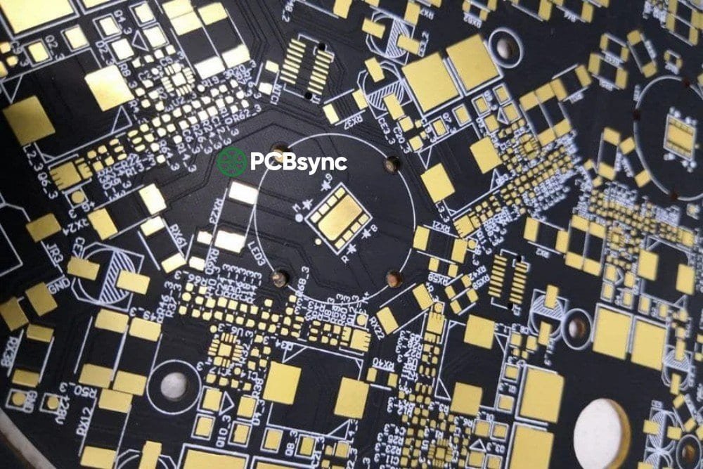
Green bare circuit board with a dense pad array and plated hole locations.
At a glance: PCB back drilling removes an unused portion of a plated via barrel with a controlled secondary drill operation. The manufacturing task is to reduce the unwanted stub while retaining the required connection.
Prepare a clearer project request

PCB Back Drilling tools

PCB Back Drilling workbench

PCBSync Engineering Tools · no account required · calculations run in your browser

Mark what you have prepared

Match the scope to the decision

PCB Back Drilling: scope, limitations and evidence

Decision / stageWhat to defineEvidence or next action
Signal requirementNets, transitions and accepted channel criteriaEstablish which sites need stub removal
Layer definitionEntry side and connection layer to preserveReview a released stackup with unambiguous numbering
Radial geometryBackdrill diameter, surrounding copper and registrationReview clearance on every traversed layer
Axial geometryDatum, removal reach and combined uncertaintyAgree the stub definition and protection margin
EvidenceLocations, inspection method and reporting requirementsTie results to the drawing revision and fabrication lot
Practical engineering and purchasing guidance

Design the process around the real requirement

Select sites that need a controlled result

Start with the signal path and identify unused barrel segments that matter to the channel. Some designs can reduce the problem by changing routing layers or selecting another via construction.

For the retained through-via architecture, create a controlled map of the locations needing removal. A blanket note on every via can add work and can conflict with connections that the circuit still requires.

Make the stackup part of the quotation

For the multilayer PCB, show the physical layer sequence and name the copper connection that must remain intact. State the entry side independently for every backdrill depth family.

Layer numbering should agree across the drawing, fabrication outputs and any signal-integrity review. When a stackup revision moves the protected layer, the drilling plan must be reviewed again.

Review two different geometric budgets

Along the board thickness, the process must approach the unwanted barrel without reaching protected copper. Across the board, the larger removal tool needs clearance and registration control around the original hole.

The online workbench helps expose an inconsistent axial budget. It does not model the conical drill tip or radial tolerances, and it cannot replace the fabrication engineering review.

Buy a defined result with suitable evidence

Include the required residual-stub definition and the agreed verification method in the request. Inspection should address the features that matter to the design, with sampling and reporting specified in advance.

Ask the quote to separate the drilling scope, additional inspection and any qualification work. We can review the submitted construction and open requirements before confirming price, schedule and exceptions.

Keep the review concrete

Include these requirements in your enquiry

01

Released stackup and layer numbering

02

Via or connector pin map identifying the required sites

03

Entry side, protected connection layer and stub requirement

04

Backdrill diameter, registration and copper-clearance requirements

05

Depth datum, tolerance basis and inspection plan

06

Order quantity, fabrication files and delivery requirement

Mark unresolved items explicitly. Ask the quotation to identify proposed exceptions, required customer approvals and any inspection or special-process charges that remain open.

See the physical construction

Real boards: construction and connection details

These real photographs from the PCBSync media library show physical board construction and connection features. Appearance alone does not verify copper weight, internal via treatment, drilling depth or lot acceptance; request corresponding drawing and inspection records.

Browse the supporting pages

PCB Back Drilling guide library

2 supporting guides

Answers before requesting a quote

PCB Back Drilling FAQ

Is backdrilling mandatory above one particular data rate?

No universal data-rate threshold applies to every board. Via geometry, edge rate, materials, routing layers and channel criteria determine whether a stub matters. Evaluate the actual transition and compare available fabrication routes.

Does the depth tool calculate a machine program?

No. It subtracts an entered removal reach from a protected-copper distance and applies your combined uncertainty. Tool-tip shape, radial geometry, machine reference and the actual residual conductive stub require engineering interpretation.

Can both sides of a board be backdrilled?

Some constructions use drilling from both entry sides. Define each operation separately and verify that the required connections and the protected region remain intact. Feasibility depends on the actual stackup and process.

What affects a backdrilling quotation?

The site count, entry sides, depth families, radial clearances, required residual stub, inspection scope and order quantity all affect the review. Submit the controlled files so the quotation can identify the applicable process and evidence.

Technical links checked 3 October 2026. Apply the current documentation and project-specific acceptance requirements. Planners do not certify manufacturability or validate uploaded design files.

From planning to a reviewed quotation

Discuss your PCB Back Drilling requirements

Send the scope you want reviewed

Add your project brief or planning scenario from the tools above. Include the controlled product revision, requested quantity, required timing and open acceptance questions.

Prepare the fabrication data, released stackup, backdrill site map, entry sides, protected layers, residual-stub requirement, radial clearances and inspection scope. Include quantity and delivery requirements. Request an NDA or file-transfer arrangement before sharing restricted files.

Email: [email protected]
Phone: +86-755-23203480

Review the message and attachments before sending. An enquiry does not place an order.

Drag & Drop Files, Choose Files to Upload You can upload up to 3 files.