Contact Sales & After-Sales Service

Contact & Quotation

  • Inquire: Call 0086-755-23203480, or reach out via the form below/your sales contact to discuss our design, manufacturing, and assembly capabilities.
  • Quote: Email your PCB files to [email protected] (Preferred for large files) or submit online. We will contact you promptly. Please ensure your email is correct.
Drag & Drop Files, Choose Files to Upload You can upload up to 3 files.

Notes:
For PCB fabrication, we require PCB design file in Gerber RS-274X format (most preferred), *.PCB/DDB (Protel, inform your program version) format or *.BRD (Eagle) format. For PCB assembly, we require PCB design file in above mentioned format, drilling file and BOM. Click to download BOM template To avoid file missing, please include all files into one folder and compress it into .zip or .rar format.

PCBSync · HDI engineering & manufacturing

HDI PCB manufacturing

Plan a compact board around the BGA escape, microvia structure and production stack-up—not a layer count alone. Compare build-up options, resolve via geometry and prepare a clear HDI PCB brief for engineering review.

Construction, material availability, price and schedule confirmed after file review.

1 + 4 + 1 · six-layer HDI exampleConceptual section · endpoints connected · not to scaleL1L2L3L4L5L6hGold: copper / connected lands. Gaps: non-connected layer clearance.Process, dimensions and dielectric stack require review.L1–L2 microviaL6–L5 microvia
Illustrative HDI cross-section: outer build-up microvias and an internal buried via. This diagram is not a manufacturing record or an approved production stackup.

Key distinction: An HDI PCB uses high-density interconnect features such as microvias, fine conductors and build-up layers to connect dense components. More layers alone do not make a board HDI.

Explore the design before release

HDI PCB tools & quotation planning

Start with the constraint, then compare structures

Select the decision you are working on. These are candidates for engineering review, not automatic stackup approval.

Compare one build-up pair against a conventional escape

A shallow outer-layer transition may release routing space. Check the package escape, dielectric depth and land geometry before selecting 1+N+1.

Bring the BGA footprint, proposed layer allocation and via span table to review.

Check surface-to-inner geometry → · Plan internal subassemblies →

Work through the detailed engineering inputs

HDI PCB project tools

PCBSync Engineering Tools · calculations run in your browser · no account required

Symmetric n+N+n notation: total copper layers = N + 2n. This is not an IPC type, press-cycle count, approved stack-up or supplier capability limit.

Start with your design inputs

Example numbers are editable. Review the result and its assumptions before adding it to your enquiry.

Design tips and manufacturing decisions

HDI PCB: what to resolve before fabrication

Choose the simplest structure that routes the design

Start with the package escape and the available routing channels. A conventional through-via multilayer board may meet the requirement if the pad field and board area allow it. A single build-up pair can provide access to inner routing layers without consuming the same through-hole area on every layer. More build-up stages should solve a demonstrated routing constraint.

Compare 1+N+1, 2+N+2 and any-layer candidates using the same net classes, reference-plane needs and component placement. The build-up planner counts copper layers; it does not calculate press cycles or prove that every BGA net can escape. Ask for a proposed production stack-up before freezing the layout.

Microvia geometry and process belong in one conversation

Specify the dielectric depth crossed by each laser via, its diameter, capture and target lands, filling requirement and relationship to the next via. Stacked microvias share a vertical location; staggered microvias offset the transitions and use routing space. Neither word alone establishes reliability.

Where a via sits in a solderable pad, define the filling, capping and planarization requirements rather than writing only “via-in-pad.” Review interfaces after the expected assembly thermal exposures. Cross-sections and electrical test provide different evidence; neither should silently replace the agreed qualification plan.

Make cost comparisons on equivalent constructions

Area, quantity, copper layers, build-up structure, line/space, material and process requirements can change the quotation. Extra sequential processing and demanding registration requirements may outweigh savings from a smaller outline. Compare total fabricated and assembled cost, not just board area.

Request an itemized quotation against the same drawing revision. Separate fabrication, fill/cap work, tooling, inspection, assembly, freight and tax. Identify material and panel-utilization assumptions so alternatives can be compared on equal terms.

Evidence that helps your team approve the supplier

Request a stack-up revision showing copper and dielectric thicknesses, via span table, material identification and any proposed exceptions. Define which controlled-impedance coupons and acceptance requirements, microsection evidence, continuity/isolation results or additional reliability evidence your product needs. Tie the requested records to a board revision and production lot. Define which uniform traces each impedance coupon represents; keep via-transition validation separate.

For BGA assembly review, add the BOM, placement files, package information and expected reflow or rework exposures. The manufacturing and assembly teams should agree panelization and pad treatment before production. This page supports that handoff; it does not promise certification, minimum geometry or delivery timing for an unreviewed construction.

Compare the architecture

Which HDI construction fits the project?

CandidateWhat it describesFirst review question
Conventional multilayerThrough vias with routing and plane layersWhen escape and area allow a simpler structure
1+N+1 / 2+N+2One / two added copper layers on each side of an N-layer coreVerify each microvia span, dielectric and land
Any-layer / ELICSuccessive interconnect structures for flexible layer accessRequires a specific fabrication and qualification proposal
HDI flex / rigid-flexDense interconnects combined with flexible regionsSeparate bend, material and assembly constraints for a rigid-flex construction

IPC HDI construction types are a separate classification. Do not equate Type I/II/III with 1/2/3 build-up layers. Confirm the complete structure, not a shorthand label.

A clearer brief gets a clearer response

Four requirements for this enquiry

01

BGA pitch, pad size and escape proposal

02

Copper stack-up and via start/stop layers

03

Material, dielectric thickness and impedance

04

Quantity, assembly exposures and acceptance plan

Attach the current fabrication files and drawing revision. Mark open questions, permitted alternatives and requested delivery timing. For assembly, add BOM and placement files. Ask for exceptions and additional test costs to be identified in the response.

Make the supplier review actionable

Ask the quotation to identify the proposed construction, manufacturing exceptions and the verification included. Agree which records are required for your board revision: stackup and material identification, electrical test scope, microsection locations or additional reliability checks.

Customer drawings and reports remain confidential. Discuss NDA and file-transfer arrangements on Contact; use your own acceptance requirements to define what evidence must accompany the order.

Real physical circuits

Board details that the manufacturing review must connect

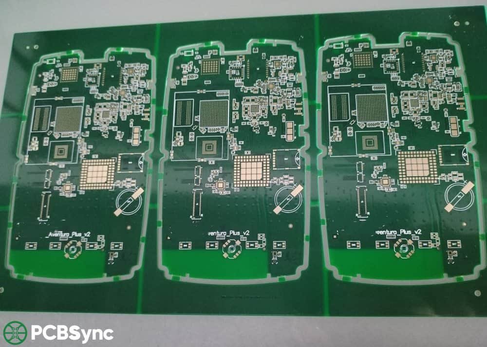
These physical PCB photographs come from the PCBSync media library. They illustrate visible pads, board outlines and panel details; they do not verify a particular hidden via structure, material grade, layer count or application qualification.

Answers for design and procurement

HDI PCB FAQ

Is HDI always cheaper than a standard multilayer PCB?

No. A smaller outline or fewer routing layers can offset some process cost, but additional build-up stages, fill/cap work, material and verification can raise total cost. Compare equivalent completed constructions.

Does 2+N+2 mean IPC Type II?

No. Build-up notation counts copper-layer additions. IPC HDI construction types describe interconnection arrangements; they are not a direct numbering of build-up stages.

What should I resolve first for HDI PCB?

An HDI PCB uses high-density interconnect features such as microvias, fine conductors and build-up layers to connect dense components. More layers alone do not make a board HDI.

Can this tool approve my design or provide a final price?

No. Geometry and allocation outputs are planning aids based on your inputs. The checklist records information prepared for review. Feasibility, material, verification scope, price and schedule require review of the actual construction.

What should I include in an HDI quotation request?

Send the current artwork and drills, outline, stack-up, via spans, quantity and requested timing. Add the material, impedance and acceptance requirements. For an assembled board, include BOM and placement data. Identify open decisions and permitted alternatives.

Technical references:NCAB: HDI structures and manufacturing · IPC: IPC-6012F scope and qualification update ↗

Supplier examples explain possible constructions; confirm project-specific limits and acceptance evidence before design release.

From planning to engineering review

Turn your HDI requirements into a clear project brief

Share what you know. Identify open decisions before committing to a production stackup.

Prepare for the discussion

  • Board revision, quantity and requested delivery date
  • Proposed stackup, material and via layer spans
  • BGA escape constraints, impedance and inspection requirements
  • Open questions and acceptable alternatives

Need an NDA or a specific file-transfer arrangement? Discuss it with us before sharing confidential files.

What should the review clarify?

  1. The proposed construction and missing information.
  2. Manufacturing constraints, material availability and verification scope.
  3. Quotation inclusions, exceptions and delivery assumptions.
Discuss my HDI project →

Submit your enquiry on Contact. An enquiry does not place an order.