Contact Sales & After-Sales Service

Contact & Quotation

  • Inquire: Call 0086-755-23203480, or reach out via the form below/your sales contact to discuss our design, manufacturing, and assembly capabilities.
  • Quote: Email your PCB files to [email protected] (Preferred for large files) or submit online. We will contact you promptly. Please ensure your email is correct.
Drag & Drop Files, Choose Files to Upload You can upload up to 3 files.

Notes:
For PCB fabrication, we require PCB design file in Gerber RS-274X format (most preferred), *.PCB/DDB (Protel, inform your program version) format or *.BRD (Eagle) format. For PCB assembly, we require PCB design file in above mentioned format, drilling file and BOM. Click to download BOM template To avoid file missing, please include all files into one folder and compress it into .zip or .rar format.

PCB manufacturing / HDI PCB / via in pad
PCBSync · HDI engineering & manufacturing

Via-in-pad PCB: specify filling, capping and BGA escape

Use via-in-pad deliberately for dense routing and define the surface condition the assembly process needs.

Construction, material availability, price and schedule confirmed after file review.

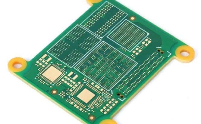
Green bare-board sample with fine-pitch pad fields and mounting holes. Internal via structure must be verified through project records.

Key distinction: A via-in-pad places a via within a component solder pad to connect to another copper layer. The name describes location; it does not by itself specify filled, capped or planarized construction.

Explore the design before release

Via-in-pad tools & quotation planning

via in pad project tools

PCBSync Engineering Tools · calculations run in your browser · no account required

Straight traces between two circular pads. This excludes via lands, diagonal escape, solder mask, pin mapping and return-path constraints. It is not a complete BGA routing solution.

Start with your design inputs

Example numbers are editable. Review the result and its assumptions before adding it to your enquiry.

Design tips and manufacturing decisions

Via-in-pad: what to resolve before fabrication

Resolve the assembly requirement first

An open hole in a solderable pad can affect solder behavior. Filled and capped constructions are used where the pad surface must support the intended assembly process, but the exact requirement must be stated.

For BGA assembly, identify the package pad geometry, finish and assembly expectations. Use the applicable via-protection terminology and drawing notes rather than relying on “VIP” alone to communicate a complete process.

Check the land around the real via geometry

A small opening still needs adequate land and alignment allowance. The BGA channel calculation is a straight-line geometry aid; a via land or anti-pad may become the actual routing constraint.

Review the microvia and component pad as part of the HDI PCB construction, with manufacturing and assembly engineers. Avoid moving a via into a pad solely to make a local CAD route possible without checking filling and surface requirements.

Include the added operations in the quote

Via filling, capping, planarization and inspection can change the manufacturing scope. Distinguish a laser microvia in a BGA pad from a larger mechanically drilled via requiring a different preparation.

Send the via family table and the expected assembly thermal history. Include these requirements in the PCB fabrication quotation and ask for exceptions before procurement compares prices.

A clearer brief gets a clearer response

Four requirements for this enquiry

01

Pad geometry, via diameter and exact location

02

Copper or resin fill / cap requirements

03

BGA escape, solder mask and surface flatness

04

Assembly process and inspection requirements

Attach the current fabrication files and drawing revision. Mark open questions, permitted alternatives and requested delivery timing. For assembly, add BOM and placement files. Ask for exceptions and additional test costs to be identified in the response.

Real physical circuits

Board details that the manufacturing review must connect

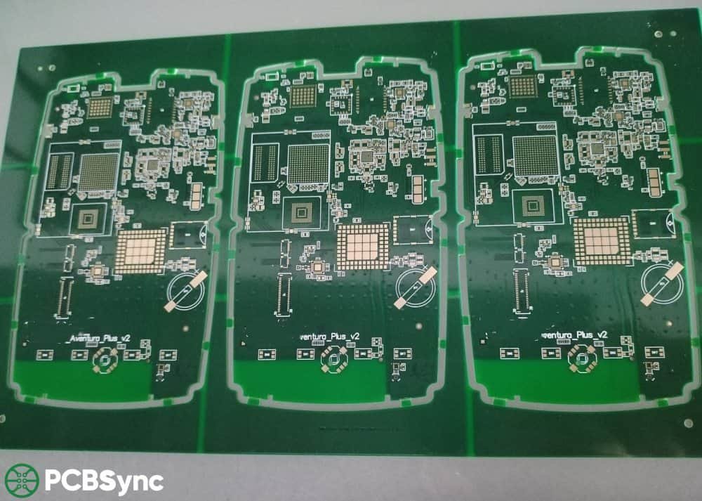
These physical PCB photographs come from the PCBSync media library. They illustrate visible pads, board outlines and panel details; they do not verify a particular hidden via structure, material grade, layer count or application qualification.

Answers for design and procurement

Via-in-pad FAQ

What should I resolve first for via in pad?

“Via-in-pad” describes location. It does not by itself specify filled, capped or planarized construction.

Can this tool approve my design or provide a final price?

No. Geometry and allocation outputs are planning aids based on your inputs. The checklist records information prepared for review. Where a budget tab is available, its uncalibrated figures are references, not order prices. Feasibility, material, verification scope, price and schedule require review of the actual construction.

What should I include in an HDI quotation request?

Send the current artwork and drills, outline, stack-up, via spans, quantity and requested timing. Add the material, impedance and acceptance requirements. For an assembled board, include BOM and placement data. Identify open decisions and permitted alternatives.

Technical references:NCAB: HDI structures and manufacturing ↗ Würth Elektronik: HDI design guide ↗

References checked 1 October 2026. Historical sources are labeled. Manufacturer examples are not PCBSync capability commitments; use current, construction-specific data for design release.

From requirements to a reviewable quotation

Discuss your via in pad project

Send the construction you want reviewed

If useful, add a planning result and your assumptions to the enquiry. Include the board revision, quantity, requested arrival date and open questions. Ask the quotation to identify the proposed stack-up, exceptions and inspection scope.

Need an NDA or a particular file-transfer arrangement? Contact us before sending files.

Email: [email protected]
Phone: +86-755-23203480

Review your message and attachments before submitting. An enquiry does not place an order.

Drag & Drop Files, Choose Files to Upload You can upload up to 3 files.