Inquire: Call 0086-755-23203480, or reach out via the form below/your sales contact to discuss our design, manufacturing, and assembly capabilities.
Quote: Email your PCB files to [email protected] (Preferred for large files) or submit online. We will contact you promptly. Please ensure your email is correct.
Notes: For PCB fabrication, we require PCB design file in Gerber RS-274X format (most preferred), *.PCB/DDB (Protel, inform your program version) format or *.BRD (Eagle) format. For PCB assembly, we require PCB design file in above mentioned format, drilling file and BOM. Click to download BOM template To avoid file missing, please include all files into one folder and compress it into .zip or .rar format.
PCB design for manufacturing connects layout decisions with fabrication, assembly and inspection. Use this guide to define the construction, resolve process questions and release an approved production package.
Project worksheet · Understand design for manufacturing and supplier review
Separate design rules from manufacturing approval.
PCB DFM asks whether the released board can be fabricated consistently with the selected process. DFA considers assembly; electrical and functional validation remain separate. Share the actual construction, not isolated minimum dimensions.
6 items still marked for review. This worksheet does not inspect files or approve a design.
What Is DFM PCB and Why Does It Matter?
Design for manufacturing connects design intent with the proposed fabrication and assembly processes. It asks whether the released geometry, materials and instructions can be produced and inspected as intended. A DRC pass checks the configured design rules; it does not establish that those rules match the supplier’s process.
Review the PCB manufacturing scope while changes are still manageable. A useful DFM response names the affected feature, explains the manufacturing concern and proposes a specific action. The design owner then decides whether the change preserves electrical, mechanical and assembly requirements.
What a DFM finding should contain
Affected layer, hole, component or drawing note, with a location that can be found in the released data.
The supplier’s process concern and the construction or tolerance on which it depends.
Proposed geometry or process change, including its effect on cost, timing and inspection.
Disposition, approval authority and the revision in which the accepted change is implemented.
Engineering queries, respins and unusable panels can affect project cost. Their frequency and cost are project-specific; a generic savings percentage is not a substitute for comparing the actual proposals.
Core DFM PCB Principles
Review a defined construction
The same trace or hole can present different manufacturing challenges in different materials, thicknesses and copper constructions. Start with the layer sequence, finished board thickness, material grades, copper and surface finish. Identify any blind, buried or laser-drilled structures and the proposed build sequence.
Review topic
Input and decision
Release evidence
Capability review
Send the actual feature and construction, rather than asking whether a standalone minimum is available.
Supplier response identifies the conditions and exceptions.
Electrical intent
Separate geometry that may be compensated from geometry fixed by impedance, timing, mating or mechanical constraints.
Approved change limits and required design-owner review.
Comparable quotations
Keep quantity, construction, inspection, reports and delivery scope consistent.
Itemized differences between the base and alternative proposals.
Understand the manufacturing sequence
PCB photoimaging and etching affect finished copper geometry. Lamination establishes the bonded construction; drilling and metallization create interlayer connections. Mask, legend and profiling complete other features. Assembly adds paste printing, placement, soldering and inspection. Review interactions across these stages instead of optimizing one feature in isolation.
Compare options without assuming the cheaper route
An extra routing layer, a different via structure or a wider trace may alter several costs at once. Request complete construction options and assess their electrical and mechanical effects before comparing quotations.
Essential DFM PCB Design Rules
Trace width and spacing
Specify the finished copper geometry needed by the circuit. Ask the fabricator to review it against copper thickness, etching and registration. Set spacing from insulation and manufacturing requirements; spacing is not universally determined by trace width. Review neck-downs, acute corners and small isolated copper features in the exported manufacturing data.
Lands and annular rings
For a circular concentric land and finished hole, half the difference between their diameters describes the nominal ring geometry. It does not account for hole displacement or establish acceptance. Define the hole and layer type, applicable criteria and registration allowances before choosing a land size. Review any teardrop additions for clearance and electrical effects; they are not an automatic requirement for every flex or small hole.
Hole structures and aspect ratio
Identify plated and non-plated holes, tool-size versus finished-hole definitions, depth and connected layers. For a through hole, thickness divided by the relevant diameter gives a geometric ratio. Whether that construction is acceptable depends on the process, materials and invoked requirements; the arithmetic alone cannot label it acceptable or problematic.
For via-in-pad, specify fill, cap and planarization requirements where needed. Review the joint and thermal-pad implications with the BGA assembly process before releasing the fabrication drawing.
Copper at the outline
Review the final outline together with routing, scoring and depaneling allowances. Distinguish a finished-board clearance from a panel clearance. Confirm intended edge plating or exposed edge contacts explicitly rather than letting them appear as accidental copper exposure.
Solder mask and legend
Check mask opening and retained-web geometry against registration and the proposed mask process. Review pad definition and paste requirements together, especially for dense packages. Keep legend out of solderable areas and verify useful reference designators, polarity and connector markings in the exported data.
For controlled-impedance circuits, the approved stack-up, copper and trace geometry must stay consistent with the drawing and CAD rules. Any proposed fabrication adjustment needs its permitted range and approval path.
DFM PCB Component Placement Optimization
Review placement for the actual PCB assembly sequence: paste printing, component access, soldering, inspection and any subsequent forming or enclosure installation.
Review topic
Input and decision
Release evidence
Component spacing
Use component-body and courtyard information, equipment access and the soldering route. Consider adjacent tall parts and connectors.
Placement review with identified interference or inspection limitations.
Orientation and polarity
Keep pin-one and polarity definitions consistent across BOM, placement and assembly drawings.
One released coordinate origin and an unambiguous assembly drawing.
Fiducials and support
Agree alignment marks, keepouts, panel handling and underside support with the assembler.
Panel/assembly drawing shows the agreed features.
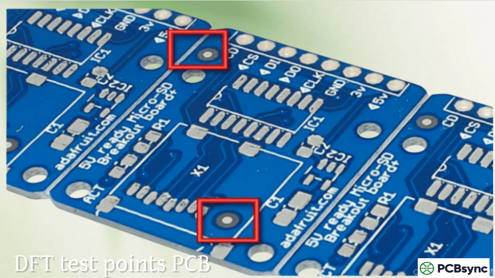
Test access
Define the selected probing or fixture approach, contact surface and access restrictions.
Test-point and fixture review linked to the assembly revision.
Do not enlarge a component pad merely to make a probe target without reviewing solder-joint effects. Where a separate test pad is proposed, check the resulting routing and parasitics as well as mechanical access.
Agree board orientation, rails, tooling, local supports and separation method with fabrication and assembly. A panel that uses material efficiently may still create handling, reflow-support or depaneling problems. Identify fragile regions and components near breakaway areas.
Acceptance data: invoked document revisions, inspection and test scope, reports and exception authority.
Revision control: identify the same approved revision across all files and record the treatment of superseded packages.
Keep required outputs explicit. A drawing note, quotation exception and CAM change should not silently describe three different constructions.
Common DFM PCB Errors and How to Avoid Them
Review topic
Input and decision
Release evidence
Hole and land mismatch
Check drill definitions, plating status and layer connectivity; resolve disagreement between drill files and drawing.
Approved drill/land changes in the released dataset.
Ambiguous mask or via treatment
Identify open, tented, filled or capped structures and their assembly purpose.
Documented treatment by via class or location.
Copper discontinuities
Review unintended islands, small features and return-path interruptions in manufacturing outputs.
Connectivity and geometry review after edits.
Assembly-access conflict
Check tall parts, connectors, soldering access and hidden-joint inspection limitations.
Agreed placement or process change.
Uncontrolled substitution
Keep proposed materials or components separate from approved alternatives.
Design-owner disposition and revision history.
Conflicting revisions
Compare fabrication, BOM, placement and test instructions before release.
A single approved package and release record.
A symptom such as bridging, tombstoning or incomplete soldering can have several causes. Review component geometry, paste, placement and thermal conditions before choosing a corrective action; one drawing change is not a universal cure.
DFM PCB Checklist for Design Review
Before layout
Identify the intended materials, layers and interconnect structures.
Obtain process feedback for unusual features and define constraints that cannot be changed.
Confirm component footprints against the relevant package documentation.
Before fabrication release
Compare the exported copper, outline and drills with the approved drawing.
Review mask, legend, edge conditions and panel arrangement.
Reconcile controlled geometry with the approved stack-up and permitted compensation.
Before assembly release
Match BOM, placement data and drawings to one revision and fitted variant.
Resolve programming, cleaning, coating and test responsibilities where applicable.
Record open exceptions and the approvals needed to start production.
A checklist records the review; it does not certify an unexamined design. For a prototype PCB assembly build, identify which questions the first build and its test plan are intended to answer.
DFM PCB Software Tools and Resources
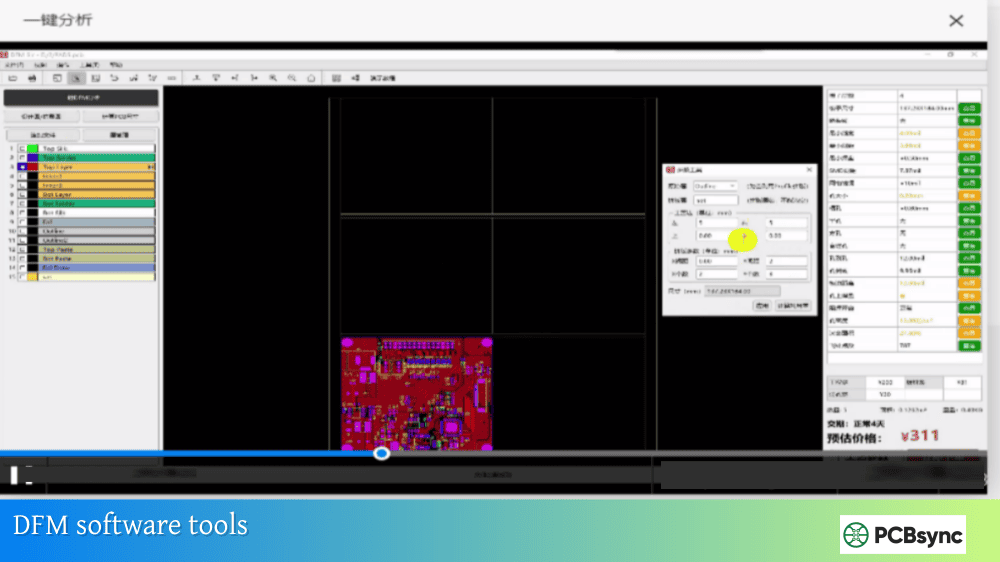
Use the CAD tool’s rule checker with constraints appropriate to the design and intended process. Review the exported files in a manufacturing-data viewer as well; export configuration and layer mapping can introduce errors that are not visible in the native design.
A software warning should be resolved against the design intent and supplier feedback. A tool’s default rule is not evidence that a particular factory or construction is qualified.
Frequently Asked Questions About DFM PCB
What is the difference between DFM and DRC?
DRC evaluates the rules configured in the design environment. DFM reviews the released design against the proposed manufacturing processes. An internally consistent CAD model can still contain an impractical construction or incomplete production instructions.
How should cost savings be evaluated?
Compare the original and proposed designs using the same quantities, acceptance scope and delivery terms. Record changes in materials, process steps, tooling and inspection. Treat a hypothetical arithmetic example as an example, not a measured customer saving.
When should the manufacturer be involved?
Review unusual constructions before routing becomes fixed. Revisit manufacturability after placement and routing, then close remaining issues against the final fabrication package. Identify whether subsequent design changes require another review.
Which findings need priority?
Prioritize issues that prevent an unambiguous build, compromise required connectivity or clearances, or require an unapproved construction change. Keep documentation gaps and process limitations visible instead of ranking them with unsupported industry percentages.
How does IPC class affect the review?
Identify the applicable document, revision, class and feature criteria. Separate bare-board requirements from assembly acceptance and product qualification. Ask what additional work the proposed scope requires; class alone is not a fixed cost multiplier or lifetime guarantee.
Useful Resources for DFM PCB Design
Consult the official IPC revision index for document status. Use the contractually invoked documents for requirements and exceptions. A public index or online summary does not supply the complete acceptance criteria.
Retain the component manufacturer’s package drawing and application guidance relevant to the design. Obtain a supplier response for the actual construction rather than copying limits from an unrelated board or generic capability table.
Implementing DFM PCB in Your Design Process
Assign responsibility for each open finding and set a release gate. The gate should show which changes are accepted, which are rejected and which remain unresolved. Update the actual production files after approval, then check that the revised package matches the disposition record.
After the build, review observed problems against the design and process records. Update the checklist with specific findings and evidence. Preserve what was learned without turning one project’s result into a universal capability or performance claim.
KEEP EXPLORING
Related engineering articles
Continue with practical guides connected to this topic.