Inquire: Call 0086-755-23203480, or reach out via the form below/your sales contact to discuss our design, manufacturing, and assembly capabilities.
Quote: Email your PCB files to [email protected] (Preferred for large files) or submit online. We will contact you promptly. Please ensure your email is correct.
Notes: For PCB fabrication, we require PCB design file in Gerber RS-274X format (most preferred), *.PCB/DDB (Protel, inform your program version) format or *.BRD (Eagle) format. For PCB assembly, we require PCB design file in above mentioned format, drilling file and BOM. Click to download BOM template To avoid file missing, please include all files into one folder and compress it into .zip or .rar format.
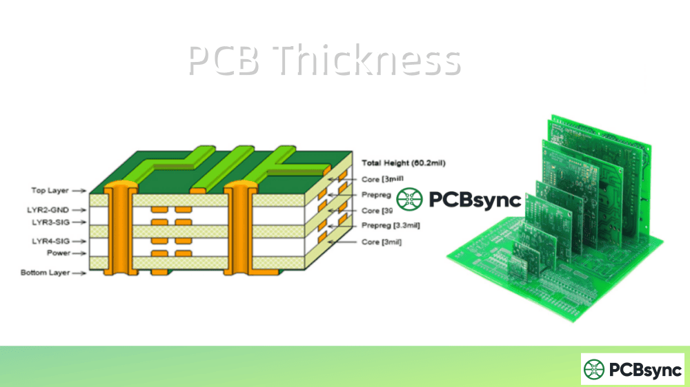
PCB thickness should follow the mechanical interface, layer construction and manufacturing requirements. This guide explains common nominal values and the checks needed before releasing a thickness specification.
Use this guide to define the mechanical envelope, review a proposed layer construction and agree inspection limits with the fabricator. Thickness selection should follow the actual enclosure, connector, electrical and assembly requirements.
PCB thickness tolerance: check the complete mechanical interval
Review updated 17 October 2026. A nominal board thickness is not a fit guarantee. State what is measured, where it is measured and which coatings are included. Separate the laminate/copper construction, local finished features, solder mask and any assembly coating. Do not assume a CAD total-thickness field and an enclosure drawing use the same convention.
The Altium Layer Stack documentation distinguishes conductive, dielectric and total thickness fields. Export the actual construction for review rather than relying only on the number shown in a summary field. For a connector, the product drawing takes priority: TE 60803-2, for example, lists a specific recommended PCB thickness range. That range is not a universal connector allowance.
Conceptual thickness budget—not a production stackup
Upper coating, if applicable ↓ Finished PCB thickness at the defined measurement location ↓ Lower coating, if applicable
Total occupied thickness = board thickness + included upper coating + included lower coating. Avoid counting the same coating twice.
Worked example: a board in a guide slot
Assume, for this fictional mechanical check, a slot width of 1.80 ± 0.05 mm and a board thickness of 1.60 ± 0.10 mm. The tightest slot is 1.75 mm and the thickest board is 1.70 mm. The worst-case total clearance is therefore 1.75 − 1.70 = 0.05 mm. This is the total clearance across the slot, not 0.05 mm on each side.
Now suppose an assembly coating is applied on both guide-contact faces, with a specified maximum of 0.03 mm per face, and was excluded from the board dimension. The maximum occupied thickness becomes 1.70 + 0.03 + 0.03 = 1.76 mm. Worst-case clearance becomes −0.01 mm: the intervals permit interference. These assumed values demonstrate the method, not a recommended coating process or production tolerance.
The nominal dimensions still appear to fit, which is why nominal-only checks miss the risk. Resolve it through a controlled change to the slot, board tolerance, coating keepout or interface design. Do not simply assume the board will stay centered, compress the coating or meet its nominal thickness.
Interface
Dimension to verify
Additional question
Card guide or enclosure slot
Minimum slot versus maximum occupied board thickness
Are mask, coating, burrs and local finish included?
Card-edge connector
Approved contact-region thickness and bevel
Does the connector drawing specify local finish and insertion geometry?
Press-fit terminal
Board thickness and finished-hole limits together
Does the compliant zone engage within the qualified range?
Drilled via
Relevant drill span and tool diameter
Does the fabricator accept the combined plating and aspect-ratio requirements?
Release checklist
Nominal thickness and explicit upper/lower limits: ____.
Measurement locations and included/excluded coatings: ____.
Mating-part minimum/maximum dimensions and drawing revision: ____.
Worst-case clearance/interference calculation and required margin: ____.
Approved stackup, material system, copper and dielectric thicknesses: ____.
Inspection method, sampling, report and deviation authority: ____.
A worst-case interval calculation is a conservative screening method. It does not replace a structural analysis, connector qualification or a statistical tolerance study with supported distributions. Thickness also does not, by itself, prove impedance or thermal performance. Keep those requirements and verification methods separate.
State the thickness measurement convention in the fabrication drawing, including the measurement location and whether solder mask, surface finish or assembly coatings are included. A nominal laminate thickness is not automatically the finished mechanical envelope.
The overall PCB thickness is determined by the combined thicknesses of several components:
Substrate/Core Material: The insulating base layer (usually FR-4 epoxy-glass laminate)
Copper Layers: The conductive traces and planes
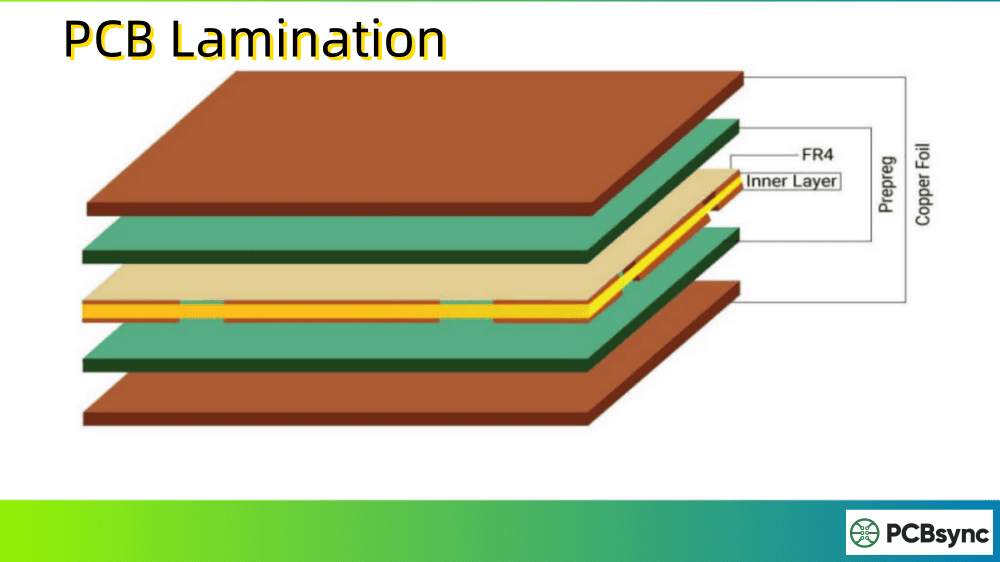
Prepreg Layers: Bonding material between layers in multilayer boards
Solder Mask: Protective coating on outer layers; confirm its local contribution and whether it is included in the specified dimension
Surface Finish: HASL, ENIG, OSP, etc. (varies by type)
Understanding this composition is crucial because each element contributes not just to thickness but also to the board’s electrical and mechanical properties.
Standard PCB Thickness Values
While there’s no official industry mandate for PCB thickness, certain values have become de facto standards due to historical reasons and manufacturing optimization.
The 1.6mm Standard: A Brief History
A nominal 1.6 mm thickness is a familiar option for rigid PCBs. It is approximately 0.063 inches or 63 mils; it is not an acceptance limit or a requirement for every board. Review the actual interface and construction before selecting it. See the circuit board manufacturing overview for release planning.
Ask whether the proposed thickness is available in the selected material and construction. Stocked options can simplify procurement, but cost and delivery depend on the complete project quotation.
Common PCB Thickness Options
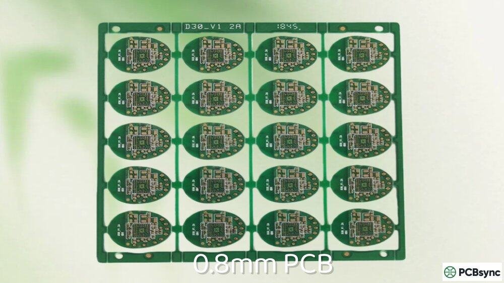
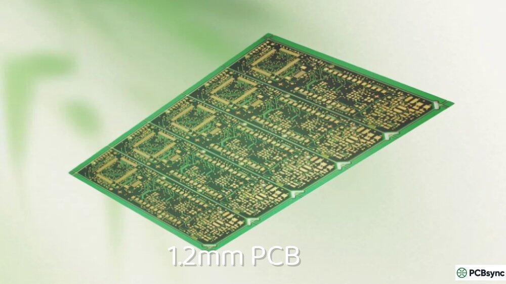
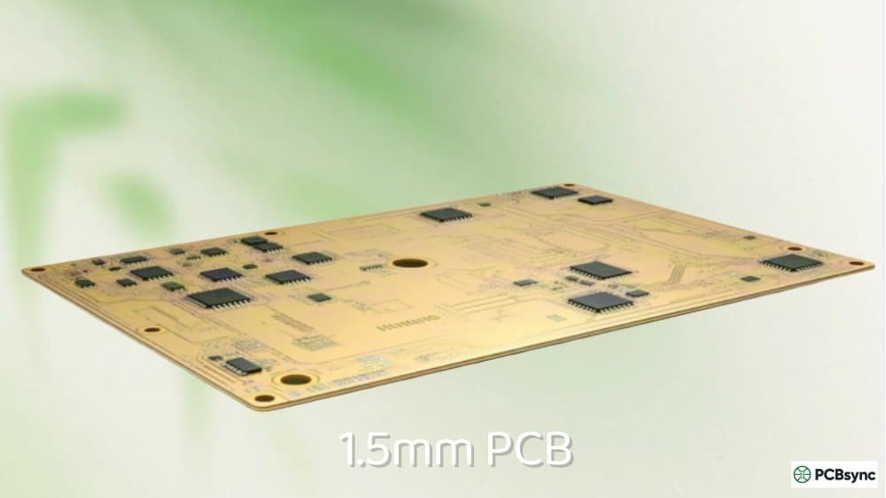
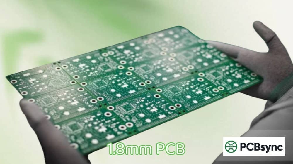
Nominal values such as 0.8, 1.0, 1.6 or 2.0 mm are examples to discuss during stackup review, not a product-to-thickness selection table. A thin rigid board is not automatically a flex circuit. Confirm the material, construction, finished tolerance and permitted bend conditions separately.
PCB Thickness by Layer Count
Layer count alone does not determine finished thickness. Build the total from the selected copper, cores and pressed dielectric construction, then check the mechanical limits. Boards with the same layer count may need different constructions because of impedance, voltage clearance, copper weight or process requirements.
Stackup review
Question to resolve
Copper layers
What starting and finished copper requirements apply?
Dielectric layers
What pressed thickness and tolerance are available for the selected material?
Total thickness
Can the proposed construction meet the defined mechanical interval?
Via structure
Are the drill span, hole size and plating requirements accepted together?
Factors That Affect PCB Thickness Selection
Choosing the right PCB thickness isn’t arbitrary—it requires balancing multiple technical and practical considerations.
Layer Count and Stackup Design
Increasing layer count adds conductive and insulating layers, but it does not impose a fixed increase in finished thickness. Review the actual material construction and copper requirements. Do not reduce copper or dielectric thickness merely to hit a nominal total without checking electrical, insulation and manufacturing requirements.
Agree the proposed stackup with the fabricator before detailed routing. Obtain the material identities, pressed dielectric dimensions, copper requirements and finished-thickness limits in a controlled drawing. Include that approved construction in the PCB release documentation and identify its revision on the fabrication order so later thickness changes can be assessed against the same mechanical interface.
Prepreg Types and Thickness
Prepreg (pre-impregnated) material bonds the layers in multilayer PCBs. Understanding prepreg options helps you achieve precise thickness targets and impedance values.
Common Prepreg Designations:
Parameter
Confirm before release
Thickness and tolerance
Actual material construction, measurement convention and agreed upper/lower limits
Material or finish data
Exact grade/process and current supplier documentation; no universal family value
Cost and availability
Project quotation and stocked constructions, not a generic percentage surcharge
Finished dielectric thickness depends on the selected resin/glass system, copper distribution and lamination process. Do not infer it from glass style alone or assume one universal direction of change with copper coverage. Ask the fabricator for the pressed construction.
Copper Weight and Thickness
Copper thickness is specified in ounces per square foot (oz/ft²), where 1oz equals approximately 35µm or 1.37 mils. Standard options include:
Copper Weight
Thickness (µm)
Thickness (mils)
Typical Use
0.5 oz
17.5
0.7
HDI, fine traces
1 oz
35
1.4
General purpose (default)
2 oz
70
2.8
Power circuits
3 oz
105
4.1
High-current applications
4 oz
140
5.5
Heavy power, busbars
If your design requires 2oz or 3oz copper for power handling, factor this into your overall thickness calculations. Heavier copper also affects minimum trace width and spacing requirements.
Heavier copper can require different trace/space allowances. Confirm the combined copper, etch geometry and spacing rules with the fabricator; a universal trace-width table is not an approval.
Substrate Material Selection
The substrate or core material forms the foundation of your PCB and significantly impacts both thickness options and electrical performance. FR-4 remains the most common choice, but other materials serve specific needs:
Parameter
Confirm before release
Thickness and tolerance
Actual material construction, measurement convention and agreed upper/lower limits
Material or finish data
Exact grade/process and current supplier documentation; no universal family value
Cost and availability
Project quotation and stocked constructions, not a generic percentage surcharge
Material selection affects the available constructions. Request the current core and prepreg options for the exact laminate grade; an FR-4 or RF material family name alone does not define available thickness, tolerance or stock status.
Signal Type and Impedance Requirements
For high-speed digital and RF designs, PCB thickness directly impacts controlled impedance. The characteristic impedance of a trace depends on:
Trace width and thickness
Distance to reference plane (dielectric thickness)
Thicker dielectric layers generally result in higher impedance for a given trace width. If you need 50Ω single-ended traces or 100Ω differential pairs, your dielectric thickness must be precisely controlled. For PCB impedance control, specify the relevant signal-to-reference dielectric spacing, material properties and trace geometry rather than relying on total board thickness alone.
Mechanical Strength and Durability
Thicker boards provide greater mechanical rigidity and resistance to flexing. This matters for:
Boards with heavy components (large connectors, heatsinks, transformers)
Designs subjected to mechanical stress or vibration
Products that must survive drop tests or rough handling
For vibration or heavy-component applications, review supports, mounting points, component loads and board strain. Greater thickness may change stiffness but does not by itself establish reliability.
Space Constraints
A compact enclosure can require a reduced board envelope. Check local component height, connector engagement, supports and assembly handling as well as PCB thickness. Where bending is required, specify an appropriate flex construction and bend requirement rather than simply thinning a rigid board.
Thermal Management
Thickness changes thermal path length and material volume, but its effect depends on the construction and heat flow. Evaluate copper distribution, vias, interfaces, heat sinks and boundary conditions rather than treating added thickness as a cooling method.
For high-power designs, consider using metal-core PCBs (MCPCBs) or incorporating thick copper layers dedicated to thermal management, rather than simply increasing overall board thickness.
Via Considerations and Aspect Ratios
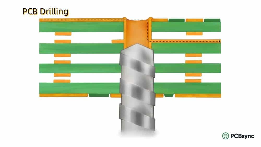
PCB thickness directly impacts via design, particularly regarding the aspect ratio—the relationship between board thickness and drilled hole diameter. This ratio affects manufacturing feasibility and reliability.
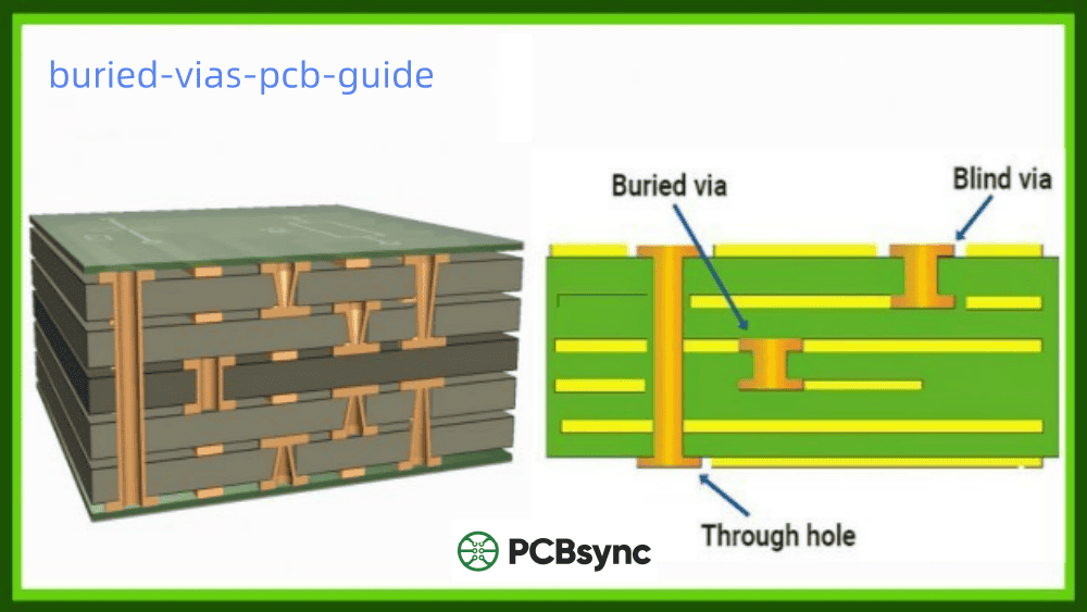
Aspect-ratio review: Use the relevant drilled span and the agreed hole-diameter convention. A through-hole spans the board; a blind or buried hole may span only part of the construction. Do not use one universal ratio limit for all via types.
For an illustrative 1.60 mm drill span and 0.20 mm drill diameter, the ratio is 1.60 / 0.20 = 8:1. This calculation does not establish whether the construction is manufacturable. Obtain acceptance for the proposed drilling, plating, material and reliability requirements.
Record each via type and its layer span.
Distinguish drill diameter from finished-hole requirements.
Confirm the process limits for the selected construction.
If a change is needed, review the electrical and mechanical effects of larger holes, a different span or a revised stackup.
Understanding how thickness affects manufacturing costs helps you make informed decisions that balance performance with budget constraints.
Cost Factors Related to Thickness
Parameter
Confirm before release
Thickness and tolerance
Actual material construction, measurement convention and agreed upper/lower limits
Material or finish data
Exact grade/process and current supplier documentation; no universal family value
Cost and availability
Project quotation and stocked constructions, not a generic percentage surcharge
Beyond the direct cost of materials and processing, non-standard thicknesses can impact other project costs:
Extended lead times: Non-stock materials require ordering, adding days or weeks
Minimum order quantities: Some materials have MOQs that increase effective cost for prototypes
Assembly adjustments: Pick-and-place machines may need setup changes for unusual board thickness
Tooling costs: Custom test fixtures may be required for very thin or thick boards
Common PCB Thickness Mistakes to Avoid
Check these common sources of specification mismatch before release.
Mistake 1: Ignoring Aspect Ratio Limits
Using a 3.2 mm drill span and a 0.2 mm drill diameter gives a 16:1 ratio. Whether that construction is acceptable depends on the actual process and reliability requirements. Confirm the span, diameter convention and fabricator approval rather than relying on a generic limit.
Mistake 2: Assuming All Fabricators Have the Same Materials
Different manufacturers stock different core and prepreg thicknesses. A stackup that’s standard at one fab house might be impossible at another. Get stackup confirmation from your chosen manufacturer before completing layout.
Mistake 3: Not Accounting for Tolerance in Enclosure Design
Use the agreed upper thickness limit in enclosure checks. A 1.60 mm nominal board reaches 1.76 mm only if the specified positive allowance is 0.16 mm; that is an example, not a universal tolerance. Include relevant coatings and local features without double counting.
Different surface finishes add varying amounts to overall thickness:
Parameter
Confirm before release
Thickness and tolerance
Actual material construction, measurement convention and agreed upper/lower limits
Material or finish data
Exact grade/process and current supplier documentation; no universal family value
Cost and availability
Project quotation and stocked constructions, not a generic percentage surcharge
Define where surface finish is present and how its local thickness affects the interface. Obtain process-specific limits for the selected finish; the finish name alone does not guarantee the completed mechanical envelope.
Mistake 5: Changing Thickness Late in Design
Changing PCB thickness after layout completion often requires re-routing impedance-controlled traces, adjusting via designs, and potentially redesigning the entire stackup. Make thickness decisions early and stick with them.
No manufacturing process is perfect, and PCB thickness will vary within specified tolerances. Understanding these tolerances helps you design boards that function correctly across the expected range.
IPC Tolerance Guidelines
Use the tolerance and acceptance conditions in the agreed drawing and applicable contract standard. Do not assume that a class designation automatically establishes ±8% or ±10% thickness tolerance.
Parameter
Confirm before release
Thickness and tolerance
Actual material construction, measurement convention and agreed upper/lower limits
Material or finish data
Exact grade/process and current supplier documentation; no universal family value
Cost and availability
Project quotation and stocked constructions, not a generic percentage surcharge
If the agreed drawing specifies 1.60 ± 0.16 mm, the resulting interval is 1.44–1.76 mm. Use the actual agreed limits in fit calculations.
Dielectric Thickness Tolerance
For impedance-controlled designs, specify the relevant signal-to-reference spacing and its construction limits separately from total board thickness. Evaluate sensitivity using the actual geometry, material data and fabrication variation. Do not assign a universal percentage tolerance or impedance shift to every stackup.
How PCB Thickness Impacts Performance
Signal Integrity
In designs with electrically significant interconnects, PCB thickness influences signal behavior in several ways:
Impedance Control: Dielectric thickness is one of the primary variables in the impedance equation. A microstrip trace on a thicker dielectric will have higher impedance than the same trace width on a thinner dielectric.
Signal Propagation Speed: Propagation depends on effective permittivity and the transmission-line geometry; thinner dielectric does not universally mean faster propagation. For timing-critical designs, consistent dielectric thickness ensures predictable propagation delays.
Crosstalk: Thicker dielectrics between signal layers and their reference planes can increase coupling to adjacent traces, potentially worsening crosstalk. Proper layer stackup design mitigates this issue.
Thermal Performance
Thicker boards don’t automatically mean better thermal management. While increased thermal mass can help with transient heat loads, steady-state thermal performance depends more on copper distribution, via design, and heat-sinking strategies.
For LED lighting applications or power electronics, consider:
Metal-core PCBs with aluminum or copper substrates
Thick copper inner layers (2oz or heavier)
Dense thermal via arrays under hot components
Mechanical Reliability
The relationship between thickness and mechanical reliability follows some general principles:
Thicker boards resist flexing and warping better than thinner ones
Specify bow and twist limits, measurement method and applicable standard revision in the order
Thinner boards are more susceptible to damage during handling and assembly
Heavy component loads can cause thin boards to sag or crack over time
For boards that will experience mechanical stress—card-edge connectors, for example—consider increasing thickness locally or throughout the design.
Choosing the Right PCB Thickness: Practical Guidelines
Use this requirement-led framework for selecting PCB thickness.
Start with the Mechanical Interface and Stackup
Begin with the enclosure and connector drawings, required layer structure, insulation requirements and assembly process. Compare available constructions against those constraints before choosing a nominal thickness.
When to Go Thinner
Consider a reduced board thickness when the following requirements justify it, subject to construction and handling review:
Space constraints require a slimmer profile
Weight is critical (aerospace, portable devices)
Flexibility is needed (certain wearables, flex-rigid designs)
Cost savings from material reduction justify potential assembly challenges
When to Go Thicker
Consider a greater board thickness when the following requirements justify it, while checking connector fit and the revised stackup:
Edge connectors or similar interfaces require specific thickness
Manufacturing Considerations
Before finalizing your thickness decision:
Check with your fabricator: Confirm they stock the materials needed for your target thickness
Review aspect ratios: Confirm each drill span and diameter against the fabricator-approved process for that construction
Factor in assembly: Confirm conveyor, support, fixture and reflow requirements for the proposed thickness and populated-board geometry
Account for warpage: Thin boards and asymmetric stackups are more prone to warping during reflow
PCB Thickness for Different Applications
Application labels do not set PCB thickness. Use the actual product requirements to identify the constraints that deserve additional review.
Application
Thickness-related checks
Portable and wearable electronics
Enclosure envelope, local supports, connector height and any flex-region bend requirement
Automotive and industrial controls
Mounting, component mass, environmental loads, assembly process and customer acceptance criteria
Aerospace and medical equipment
Controlled drawings, contract requirements, traceability and the defined qualification plan
Power electronics
Copper construction, insulation distances, thermal paths and mechanical support
RF and telecommunications
Signal-to-reference dielectric spacing, connector interfaces, material data and via geometry
If conformal coating occupies an interface region, include the specified coating interval in the mechanical check. A generic coating thickness must not replace the qualified material and process specification.
Useful Resources and Tools
Use controlled supplier drawings and current official software/material documentation when reviewing thickness.
IPC Standards Documents
These standards provide the authoritative guidance on PCB design and manufacturing:
IPC-2221 (applicable revision): Generic Standard on Printed Board Design – Covers design rules including thickness considerations
IPC-6012 (applicable revision): Qualification and Performance Specification for Rigid Printed Boards – Review the applicable requirements together with the procurement drawing; do not infer a thickness allowance from class alone
IPC-4101 (applicable revision): Specification for Base Materials for Rigid and Multilayer Printed Boards – Details laminate specifications
IPC-2141A: Design Guide for High-Speed Controlled Impedance Circuit Boards
You can purchase these standards from the IPC website (www.ipc.org) or access them through your company’s standards library.
Online Calculators and Tools
Free Tools:
Saturn PCB Toolkit (saturnpcb.com): Comprehensive Windows application covering trace width, via current, impedance, and thermal calculations
Mentor Graphics HyperLynx: Signal integrity simulation including stackup analysis
Ansys SIwave: Full-wave electromagnetic simulation for complex stackups
Educational Resources
Rick Hartley’s presentations on stackup design – Available from various PCB design conferences
Eric Bogatin’s Signal Integrity Academy – Excellent fundamentals courses
Altium Academy – Free courses covering PCB design including stackup topics
Frequently Asked Questions (FAQs)
What is the standard PCB thickness?
A nominal 1.6 mm, approximately 0.063 inches or 63 mils, is a familiar rigid-board option. It is not a universal requirement. The approved stackup and mechanical interface determine the appropriate nominal dimension and limits.
Does PCB thickness affect signal integrity?
Yes, PCB thickness significantly affects signal integrity, particularly in high-speed designs. The dielectric thickness between signal traces and reference planes directly influences characteristic impedance. A thicker dielectric increases impedance for a given trace width, while a thinner dielectric decreases it. For controlled impedance designs, precise dielectric thickness control is essential to prevent signal reflections and maintain signal quality.
How do I choose the right PCB thickness for my project?
Start with the enclosure and mating-connector limits, layer construction, copper and dielectric requirements, and assembly handling. Confirm an achievable construction with the fabricator, then specify the finished-thickness interval and measurement convention.
What is the tolerance for PCB thickness?
Thickness tolerance is an order-specific requirement. For an illustrative 1.60 mm nominal board with an agreed ±10% allowance, the interval is 1.44–1.76 mm. This arithmetic does not establish the correct tolerance for your product or IPC class.
Can I use custom PCB thickness for my design?
Yes, custom PCB thicknesses are available from most manufacturers, though they may increase cost and lead time. Fabricators typically stock specific core and prepreg materials, so custom thicknesses must be achievable by combining available materials. Contact your manufacturer early in the design process to discuss requirements and confirm feasibility before committing to a non-standard thickness.
Conclusion
A useful thickness specification joins a controlled stackup to a defined mechanical interface. Record the nominal dimension, permitted interval and measurement convention, then check electrical, assembly and mechanical requirements separately.
Remember these key takeaways:
Select nominal thickness from the actual interface and approved construction
Consider layer count, copper weight, and impedance requirements when selecting thickness
Work with your fabricator early to ensure your target thickness is achievable
Account for tolerances in your mechanical and electrical designs
Match thickness to your application’s mechanical, thermal, and electrical demands
Resolve thickness and tolerance questions before release to reduce avoidable interface and stackup changes. Reliability still requires the appropriate design review, process controls and verification for the finished product.
KEEP EXPLORING
Related engineering articles
Continue with practical guides connected to this topic.