Inquire: Call 0086-755-23203480, or reach out via the form below/your sales contact to discuss our design, manufacturing, and assembly capabilities.
Quote: Email your PCB files to [email protected] (Preferred for large files) or submit online. We will contact you promptly. Please ensure your email is correct.
Notes: For PCB fabrication, we require PCB design file in Gerber RS-274X format (most preferred), *.PCB/DDB (Protel, inform your program version) format or *.BRD (Eagle) format. For PCB assembly, we require PCB design file in above mentioned format, drilling file and BOM. Click to download BOM template To avoid file missing, please include all files into one folder and compress it into .zip or .rar format.
PCB Documentation Package: What to Include for Manufacturing
A complete PCB documentation package is the set of files and drawings that lets a fabricator build the bare board and an assembler populate it without asking you a single question. At minimum that is copper and mask data, drill files, a netlist, a fabrication drawing with stackup and notes, a BOM, a centroid file and an assembly drawing. The data files describe geometry. The drawings describe intent: which dimension is critical, what class the board is built to, what may be substituted and what may not. No data format carries intent, which is why the drawings are not optional even when your CAD output is perfect.
Here is the full package, what belongs in each part, and which standard actually governs it now.
Key takeaways
IPC-D-325 is still widely cited and dates from 1995. Current documentation requirements live in the IPC-2610 series, with IPC-2614 covering board fabrication documentation and IPC-2613 covering assembly documentation.
The drill table lists drilled sizes, not finished sizes. With roughly 1 mil of plating per wall, the finished hole comes in about 2 mil smaller, which is how press-fit connectors end up not fitting.
When the fab drawing and the CAD data disagree, the drawing usually wins. A stale drawing note can override good Gerber data.
Reference IPC standards and state your class rather than restating requirements in your notes. Restating creates conflicts; referencing does not.
Every artifact should carry the same revision identifier, and a release should always be sent as a complete set rather than as the two files that changed.
What a PCB Documentation Package Is and Who Reads Each Part
Different people in two different factories consume different parts of your release. Knowing who reads what tells you where ambiguity actually costs money.
Test is generated from the artwork, so an artwork error goes undetected
Fabrication drawing
Fab CAM and quoting
Material, finish, class and tolerances default to house standard
Stackup and impedance table
Fab lamination and CAM
Impedance is whatever the substituted construction gives you
BOM
Assembly purchasing
Wrong parts, wrong packaging, or a quote you cannot compare
Centroid / pick-and-place file
Assembly programming
Programming hours you pay for while someone rebuilds it
Assembly drawing
Assembly line and inspection
Polarity, orientation and no-populate calls get guessed
Panel or array drawing
Both
The shop panelises to its own preference, which may stress edge parts
Test and programming instructions
Assembly test
Boards ship untested or programmed with the wrong image
A useful way to think about it: the Gerber set and drill files answer “what shape is it.” The drawings answer “what matters about it.” An automated quote can be produced from the first group alone, which is why plenty of orders get placed with nothing else, and why plenty of those orders arrive built to assumptions nobody wrote down.
Is IPC-D-325 Still the PCB Documentation Standard?
IPC-D-325, Documentation Requirements for Printed Boards, Assemblies and Support Drawings, is the document most engineers name when asked which standard governs this, and it is the one still listed in plenty of company procedures and drawing title blocks. Revision A dates from 1995. IPC has since broken its content into the IPC-2610 series, which is where current documentation requirements live.
Document
Scope
When you would use it
IPC-2611
Generic requirements for electronic product documentation
The umbrella document; start here
IPC-2612
Electronic diagramming, schematic and logic descriptions
Part descriptions, discrete wiring, bill of material, process control
BOM structure and supporting documentation
Practically, most commercial fabricators will accept a package that references either, because what they need is unambiguous content rather than a particular citation. The place it matters is regulated and defense work, where a drawing citing a 1995 document as the governing documentation standard invites an audit finding that costs more to argue than to fix. Check your title block template. Many were written once and never revisited.
The Fabrication Data Set: Gerber, Drill, Netlist and Stackup
This is what the board shop needs. Send all of it, every time.
Copper, solder mask, legend and paste layers, plus the board outline on its own layer. Extended Gerber (RS-274X) is universally accepted; ODB++ and IPC-2581 carry more intelligence in a single file and reduce the chance of a layer being misidentified.
Drill files in Excellon format, with plated and non-plated holes in separate files. Slots and cutouts that are routed rather than drilled need to be dimensioned on the drawing, because they often do not appear in the drill data at all.
An IPC-D-356 netlist. Without it the fab generates its test netlist from your artwork, which means an artwork error tests as correct. This one file is the cheapest reliability insurance in the package.
A fabrication drawing with board outline and critical dimensions, drill chart, stackup, notes and title block with revision.
The stackup and, if you have controlled impedance, an impedance table naming the target, tolerance and which layers carry which structures.
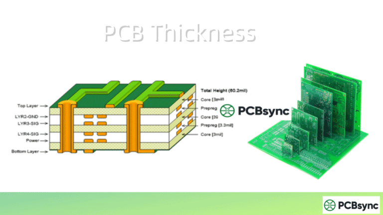
The stackup deserves more care than it usually gets. State dielectric thicknesses, copper weights per layer, material and Tg, and the total finished thickness with tolerance. If you state only total thickness, the fab is free to reach it with a different construction, and on a controlled-impedance multilayer design that substitution can move you outside tolerance while every dimension on your drawing still checks out. Name the impedance requirement and the fab will build to it and verify on a TDR coupon.
One number that catches people every year: the drill chart lists drilled diameters, and plating takes roughly 1 mil off each wall, so the finished hole lands about 2 mil smaller. Standard IPC-6012 Class 2 tolerances are around ±0.003 in (±0.076 mm) for plated holes and ±0.002 in (±0.05 mm) for non-plated. If a press-fit connector needs a specific finished hole with a tighter tolerance, that has to be called out explicitly on the drawing, hole by hole.
The Assembly Data Set: BOM, Centroid, Assembly Drawing and Test
The assembly package is where most quote delays originate, because a BOM can be technically complete and still unusable.
Artifact
What it must contain
BOM
Reference designators, quantity per board, full manufacturer part number including packaging suffix, manufacturer name, description, package, and an explicit approved-alternates column. Mark do-not-populate lines clearly, and flag MSL 2 and above
Centroid file
Reference designator, X and Y in stated units, rotation, and layer (top or bottom). State the origin and the rotation convention; these are the two things that most often need rebuilding
Assembly drawing
Component outlines with reference designators, polarity and pin 1 markings, top and bottom views, do-not-populate call-outs, hardware and any hand-assembly steps
Panel or array drawing
Array layout, rail dimensions, break-away method, and fiducials; rails should carry at least three fiducials for machine alignment
Test and programming
What gets tested, pass criteria, which image goes into which device, and where the programming file lives
Special process notes
Conformal coating and keep-out areas, torque values, serialisation and labelling, ESD or MSD handling requirements
Two BOM columns are worth arguing about internally before release. The approved-alternates column decides whether a shortage stops your build or gets solved in an afternoon, and leaving it blank means every substitution becomes an engineering query. The packaging suffix decides whether you receive reels or trays, and it is the only thing distinguishing otherwise identical part numbers.
What Belongs in Fabrication Notes and What Does Not
Notes are where designers either communicate clearly or create the conflict that stalls the job. The useful principle: reference the standard, state your class, and spell out only what is non-standard about your board.
Notes that earn their place:
The governing standard and class, for example fabricate to IPC-6012 Class 2, inspect to IPC-A-600, assemble to IPC-A-610 Class 2 and J-STD-001.
Material and Tg, surface finish, solder mask and legend colours, and whether vias are tented, plugged or filled.
Copper weights by layer, finished thickness and tolerance, and controlled impedance targets with tolerance.
Bow and twist limit; IPC-6012 sets 0.75% for boards carrying surface mount components, tested per IPC-TM-650 2.4.22.
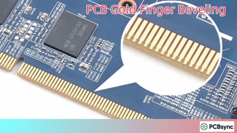
Anything that cannot be inferred from the data: castellations, edge bevels, countersinks, blind and buried via structures, back-drilling depths, UL marking requirements and the RoHS status you need.
Notes that cause trouble: restating requirements the standard already covers, which creates a conflict as soon as your wording drifts from the standard’s; notes copied from a previous project that no longer describe this board; and instructions that contradict the CAD data. On that last point, understand the hierarchy. When drawing and data disagree, most shops build to the drawing, which means a note nobody updated silently overrides correct artwork.
A customer sent a six-layer controlled-impedance design where the stackup table specified 1 oz inner-layer copper and a legacy fab note on the same drawing said 2 oz throughout. The fab built to the note. Every dimension on the drawing was correct, the boards passed visual inspection and the impedance came back outside tolerance on the differential pairs. The whole lot was scrap, and the cause was one line of text carried over from a previous project.
How to Package and Release a PCB Data Set
Release discipline is what keeps the right board getting built six months from now. Six steps.
Give every artifact the same revision identifier, and put it in the file names as well as inside the drawings.
Put the revision on the board itself if there is space. It is the only way to identify a physical board on a bench two years later.
Include a README listing every file, what it is, the units it uses, and the revision. Thirty seconds to write, and it eliminates the most common intake question.
Zip the complete set as one archive. Never send partial updates, and never send corrected layers separately, which is how boards get built from mixed revisions.
State units and origin explicitly in the README and on the drawings. Metric versus imperial confusion is rare but expensive when it happens.
Keep the released archive unchanged and start a new revision for the next change, rather than editing files inside a released package.
The honest trade-off in this whole topic: exhaustive documentation costs real engineering hours and every extra note is another opportunity for conflict. Minimal documentation is fast and hands the fab a set of decisions to make on your behalf, using its house defaults. The defensible middle is to document everything that is non-standard about your board and reference the standard for everything else. The feedback loop that tells you whether you got the balance right is the DFM report: a report full of questions means your package was thin, while one full of specific findings means the shop understood the design well enough to check it.
Common PCB Documentation Mistakes That Stall a Quote
Sending Gerbers alone for an assembly quote. Board shape is not enough to price or build a populated assembly.
Omitting the IPC-D-356 netlist, so electrical test verifies your artwork against itself.
Leaving plated and non-plated holes in one drill file.
Dimensioning slots and cutouts nowhere, because they are routed rather than drilled and do not appear in the drill data.
Specifying total board thickness without the stackup, then being surprised by the impedance result.
Reading the drill chart as finished hole sizes and ordering press-fit connectors accordingly.
Carrying over fabrication notes from a previous project, which is how a note overrides correct data.
Leaving the approved-alternates column blank, turning every component shortage into an engineering query.
Omitting the packaging suffix from part numbers and receiving trays where the line expected reels.
Sending a corrected layer instead of a complete revised package.
Citing a 1995 documentation standard in a title block on regulated work.
Frequently Asked Questions About PCB Documentation Packages
What files are needed for PCB fabrication and assembly?
For fabrication: copper, mask and legend data, separated plated and non-plated drill files, an IPC-D-356 netlist, and a fabrication drawing with stackup and notes. For assembly, add a BOM, a centroid file, an assembly drawing, and any panel, test or programming instructions.
Is IPC-D-325 still current?
It remains widely cited, and Revision A dates from 1995. IPC redistributed its content into the IPC-2610 series: IPC-2611 generic, IPC-2613 assembly documentation, IPC-2614 board fabrication documentation, IPC-2615 dimensions and tolerances. Reference the current series on regulated or defense work.
What is the difference between a fab drawing and an assembly drawing?
The fabrication drawing defines the bare board: outline, drill chart, stackup, materials, finish, tolerances and class. The assembly drawing defines what goes on it: component locations, reference designators, polarity, do-not-populate calls and any hand-assembly steps. Different factories read them.
Do I still need a fab drawing if I send ODB++ or IPC-2581?
Yes. Those formats carry stackup, netlist and drill intelligence in one file and reduce layer confusion, but no data format carries intent: which dimension is critical, what may be substituted, what class applies. That belongs on the drawing.
What should PCB fabrication notes include?
The governing standard and class, material and Tg, copper weights, surface finish, mask and legend colours, via treatment, finished thickness and tolerance, impedance targets, bow and twist limits, and anything non-standard such as castellations, bevels or back-drilling. Reference standards rather than restating them. For module edges, add castellated-hole geometry and receiving-footprint requirements so the fabrication outline and assembly interface can be reviewed together.
What happens if the drawing and the Gerber data disagree?
Most shops build to the drawing, which means an outdated note can override correct artwork. Check consistency between the two before release, particularly copper weights, hole sizes and layer counts, and delete legacy notes rather than leaving them in place.
What must a BOM include for a PCB assembly quote?
Reference designators, quantity per board, full manufacturer part number with packaging suffix, manufacturer name, description and package, an approved-alternates column, clearly marked do-not-populate lines, and MSL flags on moisture-sensitive parts. Incomplete BOMs are the leading cause of quote delays.
Releasing a Documentation Package Your Fabricator Can Build From
Good documentation is not thoroughness for its own sake. It is a short list of decisions made deliberately by you rather than by default by someone in a factory you have never visited. The package that works states the class, states what is non-standard, references the standards for the rest, and carries one revision identifier across every file in the set.
Four things worth doing this month:
Open your current fab drawing and check every note against the CAD data, especially copper weights, hole sizes and layer count. Delete anything carried over from a previous project.
Check the standard cited in your title block and update it to the IPC-2610 series if you work on regulated or defense programs.
Add an approved-alternates column and a packaging-suffix column to your BOM template and make both mandatory.
Write a one-page README template listing files, units, origin and revision, and include it in every release from now on.
Review the PCB manufacturing documentation as one controlled release: fabrication and drill data, drawing, stack-up and agreed acceptance requirements must describe the same revision. Resolve conflicts and missing information before the fabricator starts tooling.
KEEP EXPLORING
Related engineering articles
Continue with practical guides connected to this topic.