Contact Sales & After-Sales Service

Contact & Quotation

  • Inquire: Call 0086-755-23203480, or reach out via the form below/your sales contact to discuss our design, manufacturing, and assembly capabilities.
  • Quote: Email your PCB files to [email protected] (Preferred for large files) or submit online. We will contact you promptly. Please ensure your email is correct.
Drag & Drop Files, Choose Files to Upload You can upload up to 3 files.

Notes:
For PCB fabrication, we require PCB design file in Gerber RS-274X format (most preferred), *.PCB/DDB (Protel, inform your program version) format or *.BRD (Eagle) format. For PCB assembly, we require PCB design file in above mentioned format, drilling file and BOM. Click to download BOM template To avoid file missing, please include all files into one folder and compress it into .zip or .rar format.

PCBSync · Impedance engineering & PCB manufacturing

PCB Stackup Design: References, Routing & Fabrication

Build a PCB stackup around return paths, controlled structures and manufacturing constraints. Compare layer roles and thicknesses before freezing the routing rules.

Stack-up, test scope, price and schedule confirmed after file review.

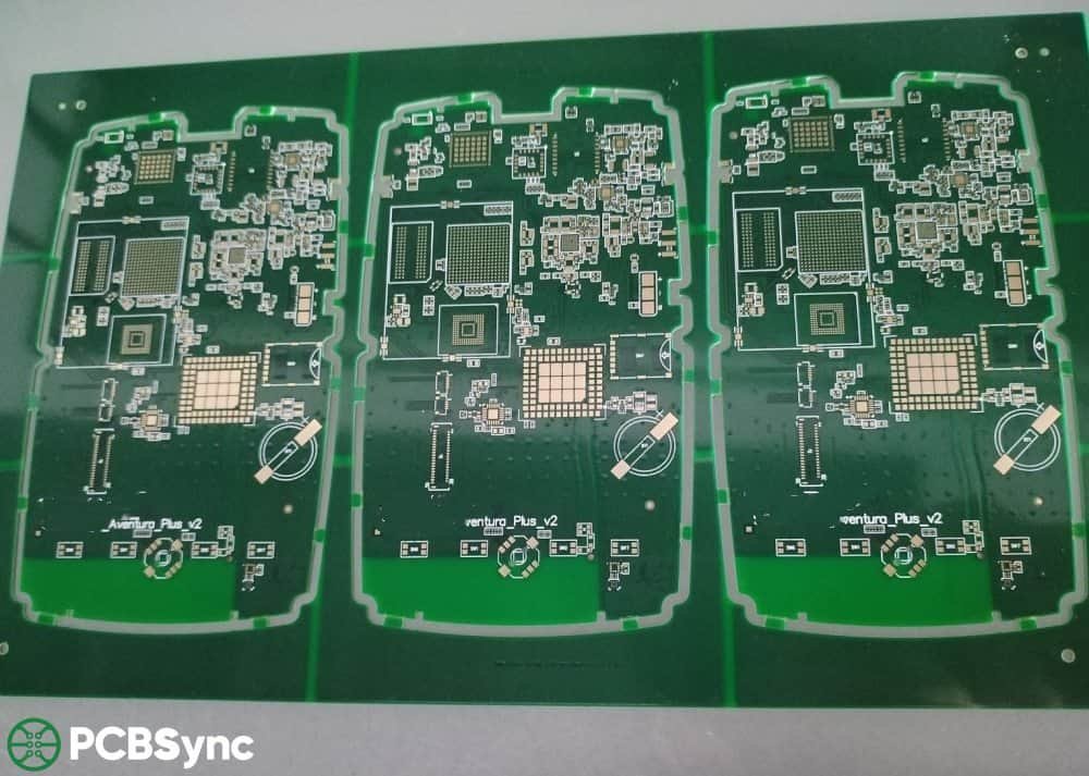
Panelized PCB sample with repeated circuits and tooling features. Review panel construction and test requirements with the fabrication files.

Key distinction: Layer count is a resource decision; reference continuity and local geometry determine whether that resource is used well.

Explore the design before release

PCB Stackup Design tools & quotation planning

PCB Stackup Design project tools

PCBSync Engineering Tools · calculations run in your browser · no account required

S = signal, G = ground, P = power, M = mixed. Enter 2–32 roles, exactly N−1 dielectric gaps, and one common copper value or N values. Dimensions in mm; coatings are not included. No stock construction is implied.

The line calculator is a separate scenario. Transfer the actual local geometry deliberately; this sketch does not assign or solve impedance automatically.

Start with your design inputs

Example values are editable. Review the result and assumptions before adding a scenario to your enquiry.

Design tips and manufacturing decisions

PCB Stackup Design: what to resolve before fabrication

Choose layer roles from the routing problem

Identify dense escapes, controlled nets, sensitive analog paths and power-distribution needs. Reserve continuous references for critical routes before filling the remaining layers. Compare alternative layer counts using actual escape and routing constraints. Carry the selected layer roles into the multilayer PCB fabrication review before fixing the routing rules.

There is no universal four- or six-layer arrangement that suits every product. A power layer used as a signal reference needs an intentional return transfer where the reference changes.

Balance electrical and manufacturing requirements

Thin reference gaps can make a useful controlled-impedance geometry possible but also affect material choices, routing width and process constraints. Finished copper and dielectric choices should be considered together. If the loss budget calls for a family such as MEGTRON 6, specify the grade, glass construction and copper option with the proposed stack-up instead of relying on the family name alone.

Review overall thickness, mechanical fit and construction balance with the fabricator. A symmetric-looking role diagram does not by itself prove balanced copper or resistance to warpage.

Publish one authoritative stack-up revision

Tie the fabrication drawing, CAD rules and simulation assumptions to the same construction. Include permitted adjustments, controlled net classes and test expectations. Define who accepts a supplier’s proposed deviation.

On a redesign, revisit connector and via transitions as well as the straight traces. Increasing layer count without updating transition models can leave the original channel problem unresolved.

A clearer brief gets a clearer response

Four requirements for this enquiry

01

Routing density and interface requirements

02

Layer roles and return references

03

Material, copper and local dielectric gaps

04

CAD rules and approved drawing revision

Attach the current fabrication files and drawing revision. Mark open questions, permitted alternatives and requested delivery timing. For PCB assembly review, add BOM and placement files, and identify any thickness or flatness constraints at component interfaces. Ask for exceptions and additional test costs to be identified in the response.

Real physical circuits

Physical PCB examples and construction details

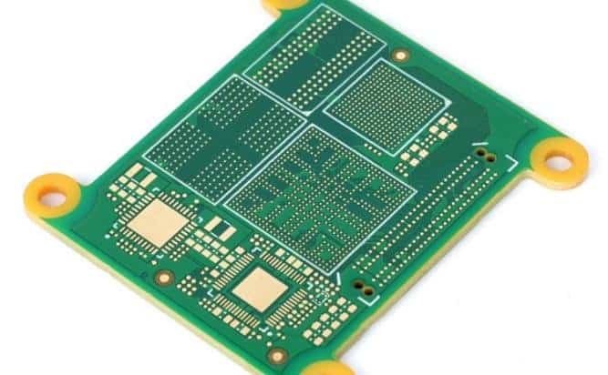
These physical PCB photographs come from the PCBSync media library. They show visible conductor patterns, pads and mechanical features. Catalog grade labels are references; photographs do not prove impedance, layer count or qualification. Confirm electrical construction through approved records.

Answers for design and procurement

PCB Stackup Design FAQ

Should I add layers to fix every impedance problem?

Not automatically. First identify whether the issue is local geometry, references, routing density or transitions. More layers may help routing while introducing other construction decisions.

Can power planes serve as references?

They can be part of a designed reference structure, but return-current transfer and power-distribution behavior must be addressed rather than assumed.

How do I request an engineering quotation?

Prepare current fabrication files, the proposed stack-up, quantity and requested delivery. Include material and inspection requirements. For controlled-impedance work, add target impedance, signal mode, controlled layers, reference planes and permitted geometry changes. Mark open questions for review. The planner is optional; you can request a quote with the information you have.

References checked 1 October 2026. Historical sources are labeled. Calculations are planning aids. Use current interface requirements, construction-specific models and agreed test procedures for design release.

From requirements to a reviewable quotation

Discuss your PCB Stackup Design project

Send the construction you want reviewed

If useful, add a planning result and your assumptions to the enquiry. Include the board revision, quantity, requested arrival date and open questions. Ask the quotation to identify the proposed stack-up, exceptions and inspection scope.

Need an NDA or a particular file-transfer arrangement? Contact us before sending files.

Email: [email protected]
Phone: +86-755-23203480

Review your message and attachments before submitting. An enquiry does not place an order.

Drag & Drop Files, Choose Files to Upload You can upload up to 3 files.