Contact Sales & After-Sales Service

Contact & Quotation

  • Inquire: Call 0086-755-23203480, or reach out via the form below/your sales contact to discuss our design, manufacturing, and assembly capabilities.
  • Quote: Email your PCB files to [email protected] (Preferred for large files) or submit online. We will contact you promptly. Please ensure your email is correct.
Drag & Drop Files, Choose Files to Upload You can upload up to 3 files.

Notes:
For PCB fabrication, we require PCB design file in Gerber RS-274X format (most preferred), *.PCB/DDB (Protel, inform your program version) format or *.BRD (Eagle) format. For PCB assembly, we require PCB design file in above mentioned format, drilling file and BOM. Click to download BOM template To avoid file missing, please include all files into one folder and compress it into .zip or .rar format.

RF & microwave · engineering to fabrication

RF PCB: from signal requirements to a reviewed build

Plan your RF PCB around the signal path, material and manufacturing stack-up. Explore design tools, compare a reference budget and send a clear fabrication enquiry.

Material, construction, price and schedule confirmed after project review.

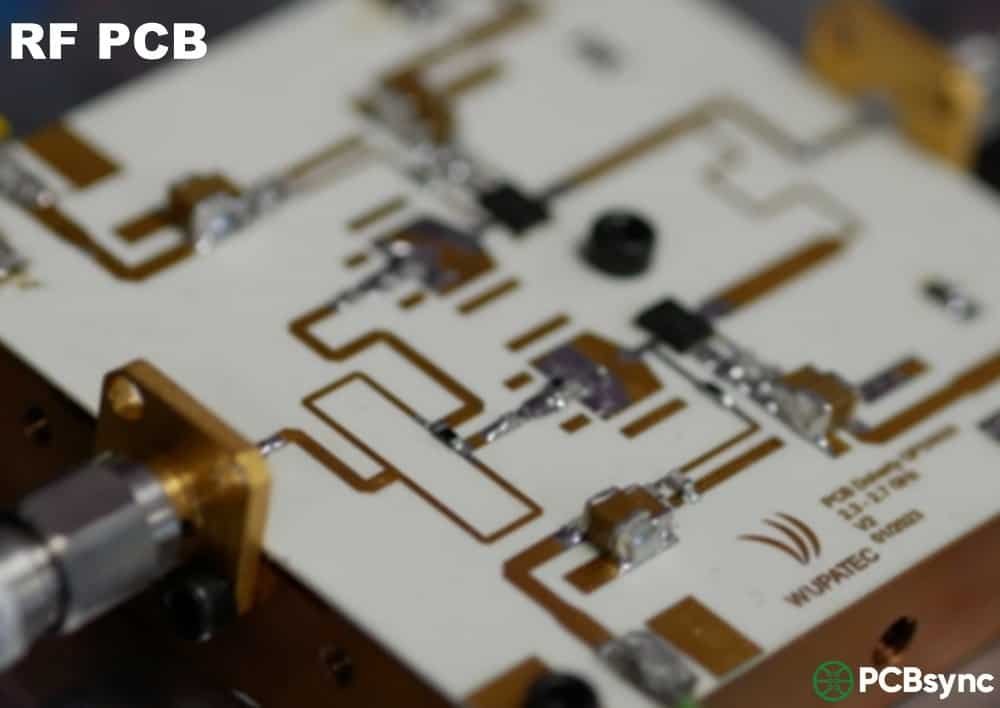
Assembled RF circuit with coaxial connectors and surface-mounted components.
Explore the next decision

RF PCB project tools

Start with a reference fabrication budget. Switch tools as needed and add the result you want reviewed to your enquiry.

RF PCB project tools

PCBSync Engineering Tools · no account required · calculations run in your browser

Existing general RF fabrication model. Material and process selections requiring review are carried into the enquiry.

Enter your project details, then calculate. You can review the result before adding it to the enquiry form.

Engineering guidance

RF PCB: decisions before release

What makes an RF PCB different?

An RF PCB carries signals for which the interconnect itself is part of the circuit. Trace geometry, reference planes, dielectric construction and transitions influence impedance, phase and loss. A board does not become suitable for RF simply because a material label says high frequency.

Begin with the operating band, bandwidth, maximum power, acceptable insertion loss and return loss. Include harmonics or fast edges that matter to the product. These requirements guide the high-frequency PCB fabrication plan, including the stack-up and validation plan; there is no single frequency cutoff that selects the correct laminate for every design.

Choose the transmission-line structure before routing

Microstrip, stripline and grounded coplanar waveguide have different field distributions and manufacturing sensitivities. Record the dielectric spacing, finished conductor geometry and adjacent copper. A 50-ohm target does not define a universal trace width.

Use the microstrip tab for a first geometry comparison only. It excludes copper thickness, solder mask, coplanar ground, roughness and dispersion. Release dimensions from the agreed production stack-up and a suitable solver, with controlled-impedance fabrication requirements recorded in the build package. Model the complete connector launch and each layer transition where their discontinuities affect the channel.

Specify the material and copper together

Compare a named laminate grade, construction, thickness tolerance and copper foil. Check whether the quoted dielectric constant is a process value or a design value, its test method and the relevant frequency. Do not compare dissipation factors taken under unrelated test conditions as if they were equivalent.

For a hybrid RF and FR-4 board, identify which layers carry RF, the bonding system and the thermal history during the multilayer construction review. Include copper roughness in the loss model and compare finishes on the actual RF geometry. Ask for proposed substitutions before manufacture, because a similar nominal Dk does not make two constructions interchangeable.

Create a continuous return path

Route the RF path with its intended reference plane. Plane gaps, long ground connections and unplanned test stubs can change the circuit. Connect surface ground and shields deliberately, and place return connections near signal layer changes using the device and connector recommendations.

A via fence is a geometry to simulate and manufacture, not a universal wavelength rule. Document via pitch, distance to the RF trace, drill size, connection layers and cavity boundaries. Keep power and digital activity from forcing RF return current around cuts or through narrow shared paths.

Make the first article answer a question

Choose the acceptance evidence before the first build: dimensional checks, material documentation, impedance coupons or specified RF measurements. An electrical continuity test establishes connectivity; it does not establish insertion loss, isolation or antenna performance.

For measured RF acceptance, define the frequency sweep, ports, reference planes, calibration and de-embedding, fixture design and limits. Before using corrected data for acceptance, check the fixture de-embedding validation evidence. Include prototype assembly conditions and enclosure conditions when they affect the result. A clear first-article plan helps distinguish a fabrication deviation from a connector, layout or system issue.

A clear brief helps the review

The requirements to put in writing

DecisionWhat to defineReview focus
SignalOperating band, power, loss and phase targetsState the performance to preserve
Stack-upNamed laminate, dielectric spacing, copper and finishAgree geometry and substitutions before release
InterconnectConnector launch, vias, shields and return pathsReview discontinuities as a complete channel
OrderQuantity, revision, arrival date and test documentsReceive a scoped engineering quotation

Define requirements for your actual construction. Tool examples do not establish material availability, production tolerances or a validated RF performance limit.

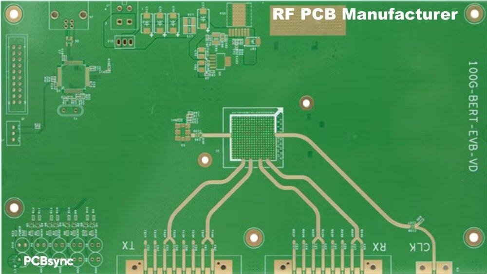
Circuit details from the media library

Physical boards and manufacturing details

Board photographs illustrate visible construction features. Material grade, internal layer count and measured RF performance require the corresponding project records.

Practical answers

RF PCB FAQ

Can FR-4 be used for an RF PCB?

Sometimes. Suitability depends on frequency, route length, loss allowance, material consistency and the circuit. Compare the specified construction and its measured or modeled performance; a frequency label alone is not enough.

Does controlled impedance guarantee RF performance?

No. Impedance is one requirement. Launches, loss, phase, coupling, component models and enclosure effects can still limit the system. Define separate RF acceptance tests where needed.

Can I request bare boards and PCB assembly together?

Yes. Include the fabrication package and, for assembly, the BOM, placement data, drawings and test instructions. Identify sensitive RF components, handling needs and any restrictions on substitutions.

Is the online budget a firm quote?

No. It uses the existing uncalibrated reference model. Material availability, hybrid construction, special processes, assembly and RF test work need file-based confirmation.

From requirements to a reviewed quotation

Discuss your RF PCB project

Send the revision you want reviewed

Include fabrication and drill data, the outline and stack-up, material grade, copper and finish, impedance notes, quantity and required arrival date. Identify critical RF geometry and any open decisions.

For RF measurements, include the frequency sweep, fixture, calibration/reference planes and acceptance limits. For assembled boards, add the BOM, placement file, assembly drawing and test instructions.

Ask for material alternatives and construction exceptions to be identified before approval. For files requiring an NDA or a particular transfer arrangement, contact us before sending them.

Email: [email protected]
Phone: +86-755-23203480

Review the generated brief and your files before submitting. An enquiry does not place an order.

Drag & Drop Files, Choose Files to Upload You can upload up to 3 files.