Inquire: Call 0086-755-23203480, or reach out via the form below/your sales contact to discuss our design, manufacturing, and assembly capabilities.
Quote: Email your PCB files to [email protected] (Preferred for large files) or submit online. We will contact you promptly. Please ensure your email is correct.
Notes: For PCB fabrication, we require PCB design file in Gerber RS-274X format (most preferred), *.PCB/DDB (Protel, inform your program version) format or *.BRD (Eagle) format. For PCB assembly, we require PCB design file in above mentioned format, drilling file and BOM. Click to download BOM template To avoid file missing, please include all files into one folder and compress it into .zip or .rar format.
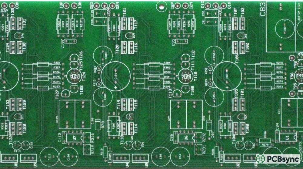
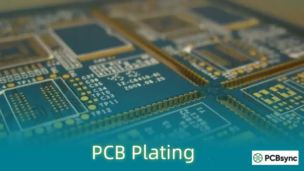
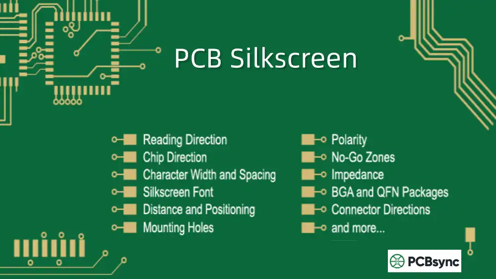
PCB silkscreen helps identify components, orientation and board revisions. Its usefulness depends on readable artwork that remains clear of exposed conductors and visible at the stages where technicians need it.
PCB silkscreen (also called the legend layer or nomenclature) is the ink layer printed on your circuit board that contains component designators, polarity markings, logos, and other human-readable information. It’s essentially the user manual printed directly onto your board, and getting it right can mean the difference between smooth production runs and costly assembly errors.
This guide covers legend materials, printing routes, layout checks and release documentation. Confirm production limits with the fabricator instead of treating a library default as a manufacturing guarantee.
PCB silkscreen is a printed information layer on a printed circuit board. It identifies parts and orientation; it is not intended to form electrical connections. Its placement and material still need review because ink on solderable surfaces can interfere with assembly.
The name comes from screen printing, but PCB manufacturing may use screen, photo-defined or digital printing processes for the legend.
Primary Functions of PCB Silkscreen
Your silkscreen layer serves several critical purposes:
Component identification — Reference designators (R1, C5, U3, etc.) help assemblers place components correctly and technicians locate parts during troubleshooting.
Polarity and orientation marking — Pin-1 and polarity indicators help communicate orientation; verify them against the component drawing and assembly documentation.
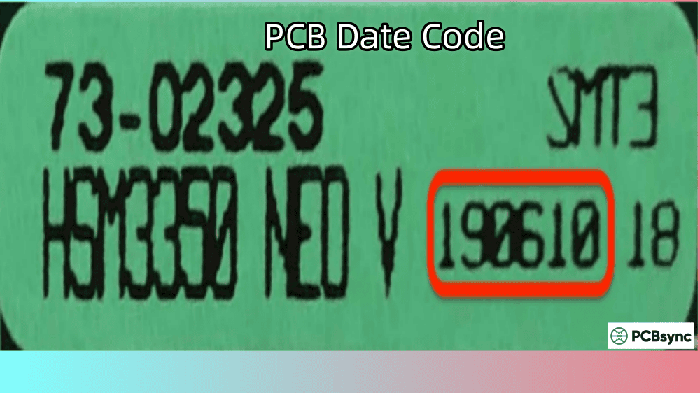
Branding and documentation — Part numbers, revisions and approved identifiers. If the board also needs a machine-readable identifier, review PCB QR code layout and readability separately from human-readable legend text. Use certification marks only when their application is authorized.
Assembly instructions — Jumper settings, configuration notes, and warning symbols.
Readable designators and unambiguous polarity marks support assembly and troubleshooting. Any claimed time saving requires evidence from the actual process; no universal percentage applies.
PCB Silkscreen Materials and Ink Types
Choose a legend ink system compatible with the board surface, the qualified cure process, soldering, cleaning and service conditions. Resin-family names alone do not establish suitability.
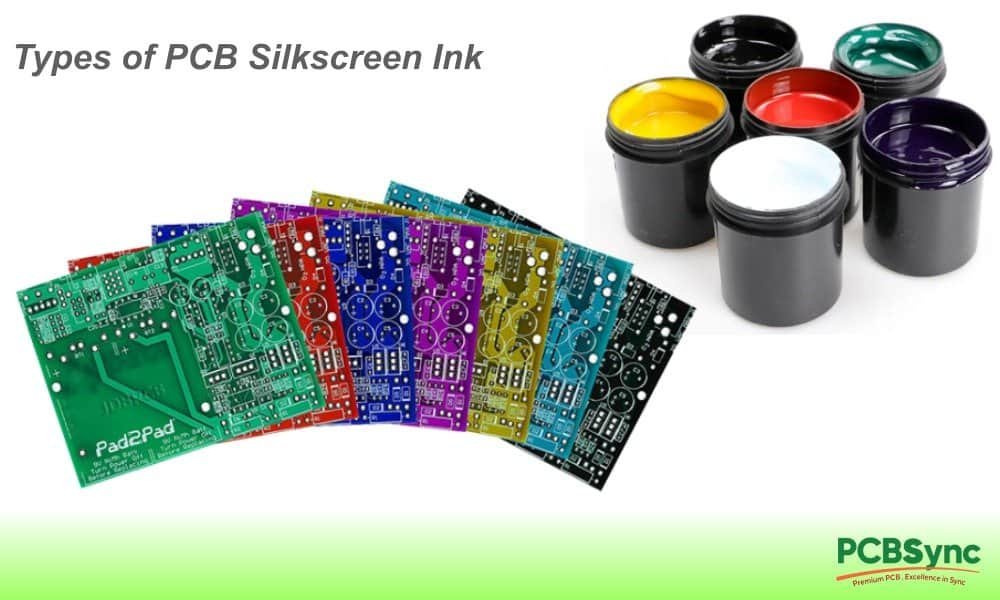
Types of PCB Silkscreen Ink
Selection item
Evidence to request
Ink product
Product identity and current technical data sheet
Cure process
Qualified thermal, UV or other specified route
Surface compatibility
Adhesion evidence on the intended surface
Process resistance
Evidence for the actual soldering and cleaning exposures
Service requirements
Agreed abrasion, chemical and readability criteria
Thermal-cure systems: Confirm the exact ink product, mixing requirements and cure schedule from its current technical data sheet. Taiyo S-200 is one manufacturer example of a thermal-cure legend ink. Confirm the material specified for your build.
UV-cure systems: UV curing is a process category, not proof of low cost or poor durability. Taiyo UVR is an example of a UV-cure marking ink. Confirm exposure, cure verification and surface compatibility for the selected product.
Material selection: Compare product-specific adhesion, chemical and thermal test evidence. Do not infer a fixed performance ranking from labels such as epoxy, acrylic or polyester.
Silkscreen Ink Properties to Consider
When specifying your PCB silkscreen requirements, consider these properties:
Adhesion strength — How well the ink bonds to the solder mask
Abrasion resistance — Important for boards that will be handled frequently
Chemical resistance — Crucial if the board will be exposed to solvents or cleaning processes
Temperature resistance — Qualify against the intended soldering and service exposure, including repeated processing where relevant.
Contrast ratio — Readability against the solder mask color
Color selection for PCB silkscreen isn’t just aesthetic—it’s a legibility issue. The goal is maximum contrast against your solder mask color for easy reading under various lighting conditions.
PCB Silkscreen Contrast Choices
Mask appearance
Contrast option to review
Dark mask
Light legend, subject to actual appearance and availability
Light mask
Dark legend, subject to actual appearance and availability
Special color or surface
Evaluate a representative sample under intended lighting
White legend is often a useful contrast choice on dark solder mask. Confirm readability using the actual color and surface finish.
Dark legend can improve contrast on light solder mask. Color availability and cured appearance depend on the ink system.
Other colors should be reviewed under the lighting used for assembly and service; color names alone do not establish contrast.
Special Color Considerations
Record application-specific requirements in the drawing rather than assuming an industry mandates one color:
Automotive: Confirm customer marking, traceability and environmental requirements.
Medical devices: Confirm which identifiers belong on the PCB and which belong elsewhere in the product documentation or labeling.
Aerospace and defense: Follow the contractually specified marking and material requirements; do not infer a color from an industry label.
Specify legend and mask colors separately. If contrast matters to a particular inspection or service task, include a review method and acceptance expectation.
PCB Silkscreen Printing Methods
How your silkscreen gets applied affects resolution, cost, and durability. Understanding the options helps you make informed decisions and communicate effectively with your fabricator.
Manual Screen Printing (Traditional Method)
The original method uses an actual mesh screen with a stencil of your artwork. Ink is pushed through the mesh onto the board surface.
Pros:
Can be suitable for repeated artwork when process setup is justified
Works well for simple designs
Confirm availability and capability with the fabricator
Cons:
Printable detail depends on screen, ink and process settings
Registration must be controlled against the specified clearances
Screen wear affects consistency
Liquid Photo Imaging (LPI)
Photo-defined legend uses an imageable material and a controlled exposure/development process. Use the selected material supplier instructions; the chemistry and processing route must not be inferred from the label alone.
Pros:
Evaluate the actual printable detail against the artwork
Process controls determine consistency
Review registration and clearance around dense footprints
Cons:
Obtain a quote for the actual artwork and quantity
More complex process
Not available at all fabricators
Direct Legend Printing (DLP) / Inkjet
Digital legend printing deposits ink directly from artwork data. It avoids a physical printing screen for that operation, but still requires setup, equipment and a qualified ink/cure system.
Pros:
Printable detail depends on the machine, ink and setup
No physical printing screen for the digital operation
Easy to change designs
Confirm registration capability on the actual construction
Evaluate setup and run cost for the requested quantity
Cons:
Adhesion must be qualified for the ink, surface preparation and cure
Not all fab houses have the equipment
May have color limitations
Select the printing route using the fabricator’s demonstrated capability, material compatibility and commercial quotation. There is no universal resolution, adhesion or cost ranking that applies to every process.
PCB Silkscreen Design Rules and Guidelines
This is where many designers get into trouble. Following proper design rules prevents manufacturing issues and ensures your silkscreen actually serves its purpose.
Critical PCB Silkscreen Design Specifications
Parameter
Release check
Text height and stroke
Agreed printable geometry and readable characters
Exposed copper clearance
Mask opening, registration allowance and agreed DRC rule
Via clearance
Actual open or covered via state
Board-edge clearance
Profile and fabrication tolerances
Reading direction
Top and bottom viewing convention
Component obstruction
Visibility where assembly or service requires it
Font Selection for PCB Silkscreen
Choose a font that remains readable at the released size and is reproduced correctly in manufacturing data:
Recommended fonts:
Stroke or vector artwork — Verify stroke width and conversion in the exported file
Simple letterforms — Check that similar characters remain distinguishable at actual size
Monospace fonts — Useful when fixed character positions help interpretation
Fonts to avoid:
Serif fonts (fine details get lost)
Script or decorative fonts
Fonts with very thin strokes
Fonts that lose detail or change geometry during export
Use a supported EDA font and inspect the exported geometry. A font that looks correct in the editor can still require manufacturing review.
Reference Designator Placement Guidelines
Place designators so their association and reading direction are clear:
Place designators adjacent to their component, not on top of it
Maintain consistent orientation — Define a reading convention suitable for assembly and service access
Group related designators — Keep them close but not overlapping
Prioritize readability — If space is tight, prioritize key components
Consider assembly process — Place designators where they’ll be visible after component placement
For dense boards, you may need to make hard choices about what gets labeled. In these cases, prioritize:
Polarized components (ICs, diodes, electrolytics)
Adjustment components (potentiometers, switches)
Test points
Connectors
What to Include on Your PCB Silkscreen
Every board is different, but there are standard elements that should appear on most designs.
Essential PCB Silkscreen Elements
Component reference designators — R1, C5, U3, etc. Follow the schematic naming convention.
Version information — Hardware version, firmware compatibility notes
Assembly notes — “NO CLEAN” indicators, special instructions
Functional labels — INPUT, OUTPUT, POWER, USB, etc. on connectors
Common PCB Silkscreen Mistakes to Avoid
Check the following failure modes before release.
Mistake #1: Silkscreen Over Pads
This is the cardinal sin of silkscreen design. When silkscreen ink gets on exposed copper pads, it can:
Prevent proper solder wetting
Cause intermittent connections
Lead to solder joint failures
The fix: Configure silkscreen clearance checks using the agreed manufacturing rules and review the plotted result against mask openings and exposed copper.
Mistake #2: Text Too Small to Read
Designers often try to label every component on a dense board, resulting in text so small it’s useless.
The fix: If text cannot meet the agreed readable size, consider:
A missing or ambiguous polarity mark can leave orientation unclear. Check it against the component drawing and assembly data rather than relying only on the footprint appearance.
The fix: Always include polarity indicators for:
All polarized capacitors
Diodes (show cathode)
ICs (pin 1 indicator)
Connectors with key orientation
LEDs
Mistake #4: Silkscreen Over Vias
Printing across an open via can interrupt the artwork or introduce ink into the opening. Review the mask state and clearance; possible issues include:
Incomplete ink coverage
Messy appearance
Potential contamination issues
The fix: Maintain the agreed clearance from exposed vias. Choose via covering for the board requirements, not merely to make an overlapping legend printable.
Mistake #5: Inconsistent Text Orientation
Boards where some text reads left-to-right, some bottom-to-top, and some upside-down are frustrating to work with during assembly and debugging.
The fix: Establish a consistent reading direction and review both board faces in their intended viewing orientation.
Mistake #6: Forgetting the Second Side
Many designers focus on the top silkscreen and forget the bottom layer entirely. If you have bottom-side components, they need proper labeling too.
The fix: Review both silkscreen layers before releasing your design.
Mistake #7: Non-Manufacturing-Ready Artwork
Silkscreen that looks great on screen may not translate to production. Common issues include:
Lines thinner than the fab house can produce
Unexpected geometry changes during text conversion or plotting
Missing clearances at board edges
The fix: Always generate Gerber files and review them with a Gerber viewer before sending to manufacturing.
Questions to Confirm with Your Fabricator
Create a release checklist using the selected fabricator’s current capability statement. Use the following questions to document the agreed requirements:
Question
Record in the release
Which process will print the legend?
Agreed process and material requirements
What geometry is supported?
Current stroke, text and clearance limits
What may CAM modify?
Approval path for clipping or moving artwork
How is readability checked?
Agreed inspection method and acceptable deviations
Do both sides need legend?
Side-specific artwork and color notes
Always check your specific fabricator’s design rules before finalizing your layout. Capabilities vary, and what works at one shop may cause problems at another.
PCB Silkscreen and IPC Standards
Identify the standards and revisions explicitly invoked by the drawing or purchase requirements. This article does not reproduce their acceptance clauses or establish certification.
Relevant IPC Standards for PCB Silkscreen
IPC-A-610 addresses electronic assembly acceptability. Verify the applicable clauses and revision rather than treating it as a universal legend manufacturing rule.
Identify which requirements apply to the delivered assembly
Record any drawing-specific marking requirements
Agree the inspection and disposition process for deviations
IPC-2221 is a generic printed-board design reference. Confirm the applicable edition and requirements for the design under review.
Specify the required identifiers
Record agreed geometry and legibility criteria
Review placement against the actual board and assembly
IPC-6012 addresses rigid printed-board qualification and performance. Use the actual invoked requirements when defining the fabrication acceptance plan.
Identify the specified board class and applicable requirements
Agree required inspection or testing evidence
Document acceptance criteria and authorized deviations
A class designation does not justify inventing numerical legend tolerances. Read the controlled requirement and identify the inspection evidence needed for this build.
Useful PCB Silkscreen Resources and Tools
The following resources can support the release review:
Design Guidelines and Standards
IPC Designer Certification Program — www.ipc.org — Training and certification for PCB design
KiCad library guidance — Silkscreen layer conventions describe reference designators, orientation marks and avoiding exposed copper. These are library conventions; confirm fabrication limits separately.
Manufacturer Design Rules — Always download and review your fab house’s specific capabilities
Gerber Output Review
Viewer type
Purpose
EDA Gerber viewer
Inspect plotted layers independently of the layout editor
Independent Gerber viewer
Cross-check the exported artwork
Ucamco reference tools
Check interpretation against the Gerber format documentation
EDA Software with Silkscreen DRC
KiCad — Review board constraints and available silkscreen checks for the version in use
Altium Designer — Configure supported manufacturing rules and inspect output
Other EDA tools — Confirm the installed version supports the required artwork export and checks
OrCAD/Allegro — Review available constraints and the released manufacturing data
Additional Reference Materials
Saturn PCB Design Toolkit — Free calculator for various PCB parameters
Footprint libraries — Verify legend geometry against the actual component and board requirements
Land-pattern references — Use the applicable controlled document and footprint guidance rather than assuming every library symbol is release-ready
PCB Silkscreen for Different Applications
Translate product requirements into a reviewable legend specification. The following are planning questions, not universal regulatory rules:
Consumer Electronics
Identify the information needed for assembly and service
Include only the approved product identifiers and necessary orientation marks
Choose contrast appropriate to the actual mask and lighting
Compare suitable printing routes with the fabricator
Medical Devices
Determine whether PCB-level traceability is required by the product documentation
Specify lot or serial fields only as required by the traceability plan
Define how readability will be inspected
Identify any required material qualification evidence
Automotive
Specify the actual soldering and service temperature exposure
Agree adhesion and cleaning compatibility requirements
Record customer-specific quality documentation requirements
Do not infer PCB marking requirements from component qualification labels
Aerospace and Defense
Identify contractual standards and revisions
Specify required material and process records
Agree the required board and assembly acceptance criteria
Check compatibility with any specified coating process
Frequently Asked Questions About PCB Silkscreen
Can PCB silkscreen be removed or modified after manufacturing?
Marking correction needs an approved rework method. Abrasion, solvents or overprinting can affect the substrate, mask or readability; evaluate the proposed method and inspect the result. Decide between controlled correction and replacement against the build requirements.
Does PCB silkscreen affect electrical performance?
The legend is intended as information rather than a conductor. It can still affect assembly if ink contaminates solderable areas or the material is incompatible with the process. Confirm clearances, cure and material compatibility instead of assuming all inks are electrically or chemically irrelevant.
What’s the minimum feature size for PCB silkscreen?
Obtain minimum stroke width, text size, registration and clearance requirements for the actual process. Check readability as well as printability. Software defaults and generic online tables are not evidence of a particular fabricator’s capability.
Should I put silkscreen on both sides of the PCB?
Use legend on each side where it serves assembly, inspection or service. Confirm the cost and availability in the quotation, and provide an assembly drawing for information that cannot fit legibly on the board.
How do I specify silkscreen color in my fabrication notes?
State solder mask and legend colors for each required side in the drawing or order data. For example, specify green mask and white legend on both sides when that is the intended construction, then check that the order and manufacturing files agree.
Conclusion
A useful legend is accurate, readable and consistent with the assembly documentation. Treat its review as part of the manufacturing release rather than a cosmetic final step.
The key takeaways:
Choose appropriate ink and color combinations for your application and solder mask
Follow design rules — minimum sizes, clearances, and placement guidelines exist for good reasons
Include the required information — Designators, orientation and approved identifiers
Avoid common mistakes — especially silkscreen over pads and illegible text
Verify before manufacturing — review Gerbers carefully, including both top and bottom silkscreen layers
Check the legend from the perspective of assembly, inspection and service. Its purpose is to make component identity and orientation clear without obstructing the features needed to manufacture the board.
For a quotation or DFM review, supply the fabrication data, assembly drawing and any special marking requirements together. Include the legend layers in the controlled PCB documentation package and identify the approved drawing revision so a corrected marking is not lost between quotation and production.
KEEP EXPLORING
Related engineering articles
Continue with practical guides connected to this topic.