Contact Sales & After-Sales Service

Contact & Quotation

  • Inquire: Call 0086-755-23203480, or reach out via the form below/your sales contact to discuss our design, manufacturing, and assembly capabilities.
  • Quote: Email your PCB files to [email protected] (Preferred for large files) or submit online. We will contact you promptly. Please ensure your email is correct.
One place for your enquiry

Continue on Contact

  1. Download the planning worksheet and review the open items.
  2. Send your requirements and available fabrication files on Contact.
  3. Agree the construction, inspection scope and quotation before ordering.
Request a project review →

Need an NDA or a particular file-transfer method? Contact us before sharing confidential files.

Notes:
For PCB fabrication, we require PCB design file in Gerber RS-274X format (most preferred), *.PCB/DDB (Protel, inform your program version) format or *.BRD (Eagle) format. For PCB assembly, we require PCB design file in above mentioned format, drilling file and BOM. Click to download BOM template To avoid file missing, please include all files into one folder and compress it into .zip or .rar format.

BGA escape, routed net classes and power-domain allocation

16 Layer PCB: Plan BGA Escape Around the Actual Nets

A 16 layer PCB can provide room for dense package escape and several routing classes, but sixteen copper layers do not guarantee a routable design. The useful starting point is the actual ball map, enabled interfaces, package locations and fabrication geometry. Build a net-class plan before approving the stackup or requesting a production quotation.

Design decisions · Construction review · Fabrication & assembly planning

16-layer BGA and net-class planning conceptPlanning illustration: 16-layer BGA and net-class planning concept. Read the labelled review points below the figure. This is not an approved manufacturing stackup.16 LAYERS / PLANNING CONCEPTExact ball mapCritical interfacePower accessVia familyEscape constraints set the allocation
  • Exact ball map
  • Critical interface first
  • Power access
  • Via-family span

Planning illustration. Geometry and layer roles require project review; no dimensions or process approval are implied.

16-layer BGA and net-class planning concept. Engineering illustration; the layer count does not establish a qualified manufacturing process.
Define the project

16-Layer BGA and Net-Class Planner

Configure the board and prepare your design questions. This custom layer count uses an engineering quotation. The tool prepares a specification and decision brief without inventing a price.

Engineering worksheet · no sign-up

Package-to-routing allocation

Allocate the active interfaces before treating sixteen layers as a solution. A completed worksheet does not prove routability.

Enable JavaScript to use this worksheet. You can also send your requirements through Contact.

Discuss this project →

Inputs stay in this page until you download them. Nothing is submitted automatically. Review the worksheet, then attach it on Contact.

WORKED ENGINEERING EXAMPLE

Separate routing-bank allocation from via approval

Hypothetical design scenario · Original conceptual diagram · Not a customer case or approved fabrication specification

Separate routing-bank allocation from via approval. Original conceptual engineering diagram; hypothetical values.01Bank A: route + reference02Bank B: route + reference03Bank C: route + reference
Bank A: route + reference · Bank B: route + reference · Bank C: route + reference. Diagram is not to scale.

A hypothetical sixteen-layer board groups interfaces into three routing banks. Each bank needs references and a way to enter and leave through a defined via family. Assigning a bank to an internal layer does not establish that its breakout, return path or residual stubs are acceptable.

Use this in your design review

  1. Name each bank and its intended layer range.
  2. Map the permitted via family for transitions into that bank.
  3. Flag reference changes, stubs and inaccessible escape regions for review.

What to bring to the review

Request a stackup and via-span drawing that use the same layer names as the layout. Avoid releasing separate documents with conflicting layer conventions.

Discuss this construction →
Board specifications, layer concepts & fabrication brief
PCBSync engineering workbench

16 Layer PCB design & cost planner

Plan the board. Compare the construction. Prepare a useful RFQ.

Enable JavaScript for the planner, or use the Contact page. No sign-in or design-file upload is needed to explore the tool.

01 / Your board specification

02 / Electrical structure

Compare the role of each copper layer before committing to a layout. Coloured rows show electrical assignments, not dielectric dimensions or a pressed stackup.

Confirm material grade, copper, dielectric spacing, impedance and tolerance with engineering. Extra layers alone do not guarantee a continuous return path.

Electrical concept

Signal / ground / power · not to scale

Engineering limits and data storage

This tool prepares specifications; it does not inspect files or issue a price, approved stackup, impedance result or delivery commitment. Non-personal specifications may be retained in this browser tab for two hours. Download and review your brief before sending it through Contact.

Package evidence

Start with the populated ball map, not only pitch

Collect the exact package drawing and the enabled pin assignment. Two devices with the same ball pitch can have different signal populations, ground locations and open escape channels. Count the active nets by bank and interface, then identify where those nets need to leave the package. Preserve the distinction between unused balls and balls that must connect to power or ground.

A small escape study should use the candidate pad, via, annular-ring and clearance rules. Route a representative difficult region before committing to the full board. Include neighboring component keepouts and decoupling access. A drawing that only routes a few outside rows does not demonstrate that inner rows can reach the proposed sixteen-layer routing plan.

  • Record package part number and drawing revision.
  • Identify optional interfaces and legal pin swaps before layout approval.
Electrical allocation

Give each routing class its own constraints

Separate memory groups, serial links, clocks, control nets and sensitive analog connections. For every class, record the allowed layers, reference conductor, impedance target where applicable, permitted transitions and the device-specific length or timing rules. Do not use a single generic high-speed rule for every signal leaving the BGA.

Reserve routes with the least flexibility first. A routing-class table helps the reviewer see conflicts early: two interfaces may require the same corridor, or a power island may interrupt an intended reference. Give mixed signal-and-power layers explicit regions in the data so that a nominal plane is not assumed continuous where the actual copper is split.

16-Layer BGA and Net-Class Planner

  1. Package data available
  2. Most constrained net class
  3. Escape demonstration
  4. Power and decoupling access
  5. Proposed via approach

Work through these decisions in the planner. Keep the resulting brief attached to the same project revision.

A review sequence for this 16-layer project. Selections in the tool create your own brief.
Net classPlan before general routingReview evidence
Memory interfaceGroup assignment and referenceDevice guide plus routed group
Serial linksChannel layers and transitionsLoss budget and via geometry
Clock or sensitive netSeparation and return pathAnnotated route
Control netsRemaining escape channelsCompleted connectivity
Access between layers

Choose the via construction from the escape study

Through vias, blind or buried vias and microvias consume different routing space and require different fabrication sequences. Compare the geometry of each useful option in the same BGA region. Include pads and antipads on the layers the hole crosses; unused drill barrels can obstruct inner routing even when the signal connects elsewhere.

Do not prescribe HDI just from ball pitch or sixteen-layer count. If via-in-pad is proposed, define the fill, cap and finished pad requirements with both fabrication and BGA assembly teams. If a buried connection is proposed, show its start and end layers and ask the supplier to identify the corresponding subassembly. The quotation should cover the selected structure, including its qualification scope.

  • Use a via-family identifier for every distinct span or construction.
  • Carry the reviewed dimensions into layout rules rather than relying on a capability-table minimum.
Power domains

Reserve power and return connections during escape

An apparently successful breakout can leave too little room for power vias or nearby decoupling. Mark the supply domains, current paths and capacitor access while the package escape is still flexible. Keep the power-distribution review tied to the device's requirements, including voltage-drop and noise limits where specified.

Consider how the package ground and supply connections reach their intended planes, and how the routing references change along each interface. More plane layers can help organization but are not a substitute for adequate interconnections and a reviewed power network. Balance the routing plan with assembly access on the opposite side of the board when capacitors or other parts sit under the package.

Engineering quotation

Release the sixteen-layer map with a fabrication proposal

Send the supplier the layer-role table, critical breakout views, complete drill spans and material or loss requirements. For PCB impedance control, ask for a proposed stack that names the dielectric and copper dimensions used to calculate each controlled geometry. Review overall thickness against connectors and hole construction before accepting the proposal.

Keep procurement exceptions visible: approved laminate alternatives, possible outline changes, acceptable via options and the tests required at prototype release. A quote that includes blind vias cannot be compared directly with a through-via quote without explaining the layout and validation differences. Request an engineering quotation for the agreed construction; a layer-count-only price would leave those decisions unresolved.

  • Match fabrication, assembly and layout revisions.
  • Record which net classes are demonstrated and which still need routing validation.
From requirements to evidence

Connect the proposed construction to the inspection plan.

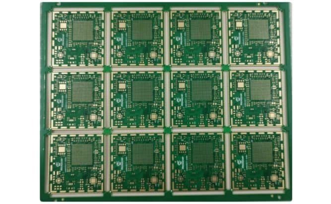
Panelized PCB sample from the PCBSync media library
PCBSync media-library sample illustrating panel format. Project-specific layer count and materials belong in the controlled fabrication record.

What should accompany the quotation?

  • Exact package and enabled pin map attached.
  • Net classes have explicit routing constraints.
  • Power and ground access appears in the escape study.
  • Every via family has a reviewed construction.

Match the quoted construction, inspection scope and delivery requirements to the released revision. Confirm what is included before placing an order.

Specific questions

16 Layer PCB questions, answered.

How many BGA balls can a 16 layer PCB support?

There is no reliable ball-count limit derived from sixteen layers alone. Active pin count, ball map, package pitch, escape geometry, board area and routing rules all matter. Demonstrate the difficult escape regions using the candidate fabrication rules.

Does a 16 layer board require blind and buried vias?

No. Through-hole construction may meet the design, while another project may need selected blind or buried spans. Choose from the actual access problem and confirm the resulting process sequence with the fabricator.

Should all high-speed nets use the same routing layers?

Not necessarily. Allocate layers by interface constraints, route length, available references and congestion. Device guidance may impose different rules on memory, serial links and clocks, even when they share one BGA.

Can the supplier pick the stackup after routing?

Material and dielectric choices affect impedance geometry and via dimensions. Obtain a proposed stack early, then control revisions. A late stack change should trigger a review of the affected routes and manufacturing rules.

What makes a sixteen-layer quotation reviewable?

It should identify the stack revision, materials, thickness, hole families, copper, controlled-impedance scope, quantity and required reports. Attach the BGA and net-class evidence so engineering exceptions have a clear context.

Engineering quotation

Request a 16-layer PCB review.

Start with the requirements you know. Include unresolved decisions so engineering can review the construction with you.

  • Exact package and enabled pin map attached.
  • Net classes have explicit routing constraints.
  • Power and ground access appears in the escape study.
  • Every via family has a reviewed construction.

Attach fabrication data, the proposed stackup and quantity breaks when ready. For assembly, include the BOM, placement data and inspection requirements.

Discuss NDA arrangements before sharing confidential files. Ask for current certification scope and records relevant to your project.

Contact PCBSync · Include PCB assembly

One place for your enquiry

Continue on Contact

  1. Download the planning worksheet and review the open items.
  2. Send your requirements and available fabrication files on Contact.
  3. Agree the construction, inspection scope and quotation before ordering.
Request a project review →

Need an NDA or a particular file-transfer method? Contact us before sharing confidential files.

PCBSync engineering resources · Updated 1 October 2026 · Planning guidance and illustrations are not approved manufacturing stackups.