Contact Sales & After-Sales Service

Contact & Quotation

  • Inquire: Call 0086-755-23203480, or reach out via the form below/your sales contact to discuss our design, manufacturing, and assembly capabilities.
  • Quote: Email your PCB files to [email protected] (Preferred for large files) or submit online. We will contact you promptly. Please ensure your email is correct.
Drag & Drop Files, Choose Files to Upload You can upload up to 3 files.

Notes:
For PCB fabrication, we require PCB design file in Gerber RS-274X format (most preferred), *.PCB/DDB (Protel, inform your program version) format or *.BRD (Eagle) format. For PCB assembly, we require PCB design file in above mentioned format, drilling file and BOM. Click to download BOM template To avoid file missing, please include all files into one folder and compress it into .zip or .rar format.

PCB manufacturing / Impedance Control PCB / Return Path Analyzer
PCBSync · Impedance engineering & PCB manufacturing

Return Path Analyzer: A Guided Layout Review Checklist

Organize your return-path review around references, discontinuities and transitions. Build an engineering brief from your observations without uploading design files.

Stack-up, test scope, price and schedule confirmed after file review.

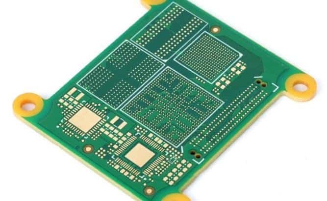
Physical PCB sample with exposed ground regions, traces and mounting holes. Confirm the material and electrical construction in the approved records.

Key distinction: This is a manual checklist, not an automatic CAD analyzer or electromagnetic simulation.

Explore the design before release

Return Path Analyzer tools & quotation planning

Return Path Analyzer project tools

PCBSync Engineering Tools · calculations run in your browser · no account required

Mark the information you have prepared after reviewing your design. This manual checklist does not analyze files or approve electrical performance.

Start with your design inputs

Example values are editable. Review the result and assumptions before adding a scenario to your enquiry.

Design tips and manufacturing decisions

Return Path Analyzer: what to resolve before fabrication

Inspect one signal path at a time

Identify the source, destination and each routing layer. Record the actual reference conductor for every segment. Mark slots, voids, dense antipad fields and connector regions that may change the return environment.

Use the checklist after viewing the relevant copper layers. A checked item means you have prepared that information; it does not mean the structure has been validated.

Explain every reference change

At each layer transition, identify whether the signal retains the same reference or moves to another one. Record the proposed return-transfer path and any remaining uncertainty.

When references belong to different nets, resolve the transfer using the system and component guidance. Do not assume a nearby ground via answers every reference transition.

Send a focused review package

For the multilayer PCB review, include annotated routing views, stack-up, interface requirements and the regions you want assessed. State which constraints can change and who owns the approval.

The generated brief can accompany your RFQ. For proof of channel or EMC behavior, agree the appropriate simulation or measurement separately from this preparation checklist.

A clearer brief gets a clearer response

Four requirements for this enquiry

01

Each segment and its actual reference

02

Plane gaps, slots and connector regions

03

Return transfer at every layer transition

04

Annotated evidence and open design questions

Attach the current fabrication files and drawing revision. Mark open questions, permitted alternatives and requested delivery timing. For assembly, add BOM and placement files. Ask for exceptions and additional test costs to be identified in the response.

Real physical circuits

Physical PCB examples and construction details

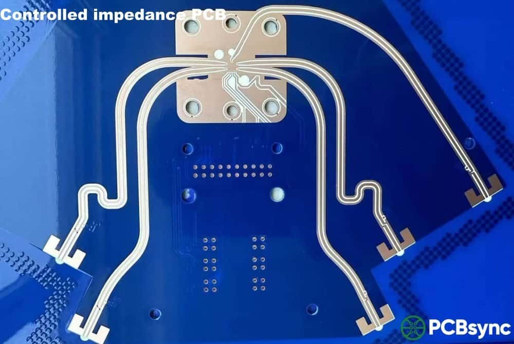
These physical PCB photographs come from the PCBSync media library. They show visible conductor patterns, pads and mechanical features. Catalog grade labels are references; photographs do not prove impedance, layer count or qualification. Confirm electrical construction through approved records.

Answers for design and procurement

Return Path Analyzer FAQ

Will this tool upload or analyze my Gerber files?

No. All interaction is a local manual checklist. Share files through an agreed quotation process when you want engineering review.

What does 6/6 prepared mean?

You marked all preparation items. It is not a score for electrical performance or approval to fabricate.

How do I request an engineering quotation?

Prepare current fabrication files, the proposed stack-up, quantity and requested delivery. Include material and inspection requirements. For controlled-impedance work, add target impedance, signal mode, controlled layers, reference planes and permitted geometry changes. Mark open questions for review. The planner is optional; you can request a quote with the information you have.

References checked 1 October 2026. Historical sources are labeled. Calculations are planning aids. Use current interface requirements, construction-specific models and agreed test procedures for design release.

From requirements to a reviewable quotation

Discuss your Return Path Analyzer project

Send the construction you want reviewed

If useful, add a planning result and your assumptions to the enquiry. Include the board revision, quantity, requested arrival date and open questions. Ask the quotation to identify the proposed stack-up, exceptions and inspection scope.

Need an NDA or a particular file-transfer arrangement? Contact us before sending files.

Email: [email protected]
Phone: +86-755-23203480

Review your message and attachments before submitting. An enquiry does not place an order.

Drag & Drop Files, Choose Files to Upload You can upload up to 3 files.