Contact Sales & After-Sales Service

Contact & Quotation

  • Inquire: Call 0086-755-23203480, or reach out via the form below/your sales contact to discuss our design, manufacturing, and assembly capabilities.
  • Quote: Email your PCB files to [email protected] (Preferred for large files) or submit online. We will contact you promptly. Please ensure your email is correct.
Drag & Drop Files, Choose Files to Upload You can upload up to 3 files.

Notes:
For PCB fabrication, we require PCB design file in Gerber RS-274X format (most preferred), *.PCB/DDB (Protel, inform your program version) format or *.BRD (Eagle) format. For PCB assembly, we require PCB design file in above mentioned format, drilling file and BOM. Click to download BOM template To avoid file missing, please include all files into one folder and compress it into .zip or .rar format.

Double-sided reference continuity and the decision to move to four layers

2 Layer PCB: Protect the Return Path

A conventional two-layer rigid PCB places copper on both faces of one insulating substrate. The second face makes crossings easier, but routing both sides heavily can fragment the ground copper. Decide whether two layers are enough by reviewing the return path as carefully as the signal trace.

Design decisions · Reference budgeting · Fabrication & assembly planning

Trace the signal and its returnPlanning illustration: Trace the signal and its return. Read the labelled review points below the figure. This is not an approved manufacturing stackup.2 LAYERS / PLANNING CONCEPTConnected groundGround interruptionSignalReturn-path review
  • Top signal route
  • Bottom ground copper
  • Ground interruption
  • Signal via
  • Reference connection

Planning illustration. Geometry and layer roles require project review; no dimensions or process approval are implied.

Trace the signal and its return. Engineering illustration; the layer count does not establish a qualified manufacturing process.
Define the project

Two-layer reference-copper audit

Configure the board and prepare your design questions. A rigid FR-4 reference base budget is available for supported scenarios; other materials and custom processes need separate quotation.

PCBSync engineering workbench

2 Layer PCB design & cost planner

Plan the board. Compare the construction. Prepare a useful RFQ.

Enable JavaScript for the planner, or use the quotation form below. No sign-in or design-file upload is needed to explore the tool.

01 / Your board specification

02 / Electrical structure

Compare the role of each copper layer before committing to a layout. Coloured rows show electrical assignments, not dielectric dimensions or a pressed stackup.

Confirm material grade, copper, dielectric spacing, impedance and tolerance with engineering. Extra layers alone do not guarantee a continuous return path.

Electrical concept

Signal / ground / power · not to scale

Budget assumptions, data storage & engineering limits

The base budget uses the same existing FR-4 model as the PCBSync manufacturing page: area, quantity, layer count, thickness, finish and outer-copper factors plus a setup allowance. The illustrative range is ±20% of that model; it is not a statistical confidence interval. Material grade, inner copper, impedance, advanced vias and other listed requirements need separate pricing. Supported rigid FR-4 scenarios with 1, 2, 4, 6, 8, 10 or 12 copper layers can show a reference budget; odd counts above one, higher layer counts and unsupported combinations request an engineering quotation.

No released stackup, impedance solution, file DFM or delivery commitment is produced. Valid non-personal specifications can be kept in this browser tab for two hours to support movement between these layer pages. Free-text notes, dates, contact details and design files are not stored by this tool. No AI API is called. Model: 2026.09.30-v3; layer planner: 2026.10.01-l2.

Construction

Two copper faces joined by defined interconnects

For a conventional rigid FR-4 design, top copper and bottom copper are separated by the substrate. A plated through-hole or via can connect the faces. A drilled hole without plating does not provide that electrical connection by itself. Describe finished hole size, pad geometry and plating requirements in the fabrication data so the board and its interconnects form one clear specification.

Copper-layer count is independent of component-side count. Components may occupy one or both faces of a two-layer PCB; double-sided assembly introduces its own placement and soldering considerations. Metal-core and flexible boards may use different arrangements, so a two-layer request should identify the construction rather than assume every two-copper-layer board uses the same cross-section.

  • Identify the top and bottom copper files and keep their origin and orientation aligned.
  • Separate plated drill data from non-plated mechanical holes.
  • Define assembly sides independently of the two-copper-layer fabrication requirement.
Return paths

Inspect the ground copper underneath each critical route

One useful starting strategy is to keep most components and critical routing on one face while preserving broad, connected ground copper on the other. The strategy succeeds only if routing, mounting holes, connector cutouts and clearances leave a usable return path. A ground pour can look extensive while narrow bridges or isolated islands undermine the intended connection.

Follow each important signal from its driver to receiver and inspect the reference region along the entire route. Pay special attention to traces passing over a gap or a long bottom-layer trace that cuts across ground. Where connected ground exists on both faces, appropriately placed stitching vias can connect those regions; they cannot create a missing plane or repair every geometric interruption.

  • Refill copper after layout changes before reviewing connectivity.
  • Inspect ground necks around connector fields and mounting holes.
  • Keep switching-power loops and sensitive measurement returns from sharing restrictive copper paths.

Two-layer reference-copper audit

  1. Bottom copper usage
  2. Critical signals change faces?
  3. Impedance requirement
  4. Package escape status
  5. Power and sensitive return interaction

Work through these decisions in the planner. Keep the resulting brief attached to the same project revision.

A review sequence for this 2-layer project. Selections in the tool create your own brief.
Routing

Use the second face without losing the reference

The routing advantage of two layers is the ability to move a signal through a via and cross another route on the opposite face. That transition also changes the surrounding electromagnetic geometry. Review where the signal's return can travel before and after the via. A nearby ground connection helps only when it joins the actual reference regions used by the route.

For power paths, the via and its connected pads belong in the current and temperature-rise review. For dense components, inspect the fanout at the real pad size, clearances and drill geometry. NXP publishes a two-layer guide for a particular VFBGA98 package; that illustrates why the actual ball map matters. It does not establish that every BGA of a given pitch works on two layers.

  • Review vias, trace necks and connector pads as one current path.
  • Mark the critical layer changes on the layout screenshot sent for review.
  • Use the component vendor's layout guidance for the actual device.
Geometry

Board thickness affects more than enclosure fit

On a two-layer board, the opposite copper face can be relatively far from a surface trace. For a chosen impedance, trace width depends on that separation, copper thickness, dielectric properties and nearby copper. A copied width from a four-layer board therefore may not apply. Coplanar ground changes the structure again and should be included in the impedance model.

If PCB impedance control is required, define the relevant net classes, target values and tolerance, then obtain an agreed construction and geometry before routing the critical region. A thinner board can change the feasible dimensions but must still meet connector, stiffness and handling requirements. Neither a nominal thickness nor the words two-layer stackup establish electrical suitability.

  • Specify finished board thickness and its mechanical tolerance.
  • Include solder mask and coplanar copper assumptions where relevant.
  • Confirm the geometry and any requested coupon verification with the fabricator.
Decision

Move to four layers when dedicated references solve the problem

Consider four layers when escape routing repeatedly cuts ground, critical signals need more predictable reference geometry, or power distribution competes with nearly every available route. Four layers can reserve internal copper for reference and power while leaving surface space for components. The benefit comes from the selected layer assignment and layout, not from the count alone.

Compare two complete designs at the same quantity and acceptance requirements. A two-layer board may be larger or take more layout effort; a four-layer board may reduce congestion but introduce different material and impedance requirements. Send both outline assumptions, the critical interfaces and a short explanation of the unresolved routing problem. This gives a meaningful basis for a quote comparison.

Observed constraintTwo-layer actionFour-layer review trigger
Ground interrupted by routesRe-place parts and shorten crossingsContinuity cannot be maintained
Dense package escapeCheck actual pad/drill/spacing geometryEscape consumes required reference copper
Controlled impedanceModel the real two-layer structureFeasible geometry conflicts with routing
Power distributionCheck copper necks and viasRouting space and return paths compete
From requirements to evidence

Connect the proposed construction to the inspection plan.

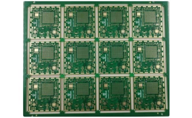
Panelized PCB sample from the PCBSync media library
PCBSync media-library sample illustrating panel format. Project-specific layer count and materials belong in the controlled fabrication record.

What should accompany the quotation?

  • Inspect connected ground after copper refill.
  • Mark critical signal layer changes.
  • Check via and pad bottlenecks in power paths.
  • Confirm impedance geometry if specified.

Match the quoted construction, inspection scope and delivery requirements to the released revision. Confirm what is included before placing an order.

Specific questions

2 layer PCB questions, answered.

Does a two-layer PCB need one complete ground layer?

It depends on the design, but preserving a broad continuous ground reference is often valuable. A practical two-layer layout may contain some routing on both faces. Review where that routing interrupts the required return paths.

Is a double-sided PCB the same as double-sided assembly?

No. Double-sided PCB commonly describes copper on both faces. Double-sided assembly means components are fitted on both faces. A two-layer PCB can have components on only one face.

Can two layers support controlled impedance?

Potentially, when the real dielectric separation, trace dimensions, copper and reference geometry support the target. Have the structure modeled and agreed; a generic trace-width value is insufficient.

When should I change from two layers to four?

When a practical two-layer placement cannot preserve required references, escape routing, power paths or electrical margin. Use routing and return-path evidence rather than a single clock-speed or component-count rule.

What files make a two-layer quote useful?

Provide both copper faces, outline, plated and non-plated drill information, mask/legend files and thickness/material requirements. Add impedance requirements and critical-net notes if applicable, plus assembly data when components are included.

Engineering quotation

Request a 2-layer PCB review.

Start with the requirements you know. Include unresolved decisions so engineering can review the construction with you.

  • Inspect connected ground after copper refill.
  • Mark critical signal layer changes.
  • Check via and pad bottlenecks in power paths.
  • Confirm impedance geometry if specified.
  • Compare a four-layer layout where the constraints remain unresolved.

Attach fabrication data, the proposed stackup and quantity breaks when ready. For assembly, include the BOM, placement data and inspection requirements.

Discuss NDA arrangements before sharing confidential files. Ask for current certification scope and records relevant to your project.

Contact PCBSync · Include PCB assembly

Drag & Drop Files, Choose Files to Upload You can upload up to 3 files.

Further engineering reading: Altium: Understanding 2-Layer PCB Ground Planes Würth Elektronik: Basic PCBs

PCBSync engineering resources · Updated 1 October 2026 · Planning guidance and illustrations are not approved manufacturing stackups.