Contact Sales & After-Sales Service

Contact & Quotation

  • Inquire: Call 0086-755-23203480, or reach out via the form below/your sales contact to discuss our design, manufacturing, and assembly capabilities.
  • Quote: Email your PCB files to [email protected] (Preferred for large files) or submit online. We will contact you promptly. Please ensure your email is correct.
Drag & Drop Files, Choose Files to Upload You can upload up to 3 files.

Notes:
For PCB fabrication, we require PCB design file in Gerber RS-274X format (most preferred), *.PCB/DDB (Protel, inform your program version) format or *.BRD (Eagle) format. For PCB assembly, we require PCB design file in above mentioned format, drilling file and BOM. Click to download BOM template To avoid file missing, please include all files into one folder and compress it into .zip or .rar format.

Single-sided routing and jumper-inclusive assembly cost

Single Layer PCB: Make One Copper Face Work

A single layer PCB has one patterned copper layer. Its value depends on whether placement, jumpers and board size keep the complete assembly simple. Use this guide to check a single-sided design before choosing materials or asking for a fabrication quote.

Before adding a jumper or moving a connector, review which side remains accessible for assembly and inspection. Include the component population and any manual operations in the handoff rather than supplying only copper artwork. See assembly process planning for the related requirements.

Design decisions · Reference budgeting · Fabrication & assembly planning

One copper face, two assembly viewsPlanning illustration: One copper face, two assembly views. Read the labelled review points below the figure. This is not an approved manufacturing stackup.1 LAYERS / PLANNING CONCEPTComponent faceCopper face / sectionFitted jumperOne copper pattern
  • Component body
  • Jumper with BOM reference
  • One copper pattern
  • Insulating substrate
  • Solder pad on copper face

Planning illustration. Geometry and layer roles require project review; no dimensions or process approval are implied.

One copper pattern and a fitted jumper. Engineering illustration; the layer count does not establish a qualified manufacturing process.
Define the project

Single-sided routing and jumper review

Configure the board and prepare your design questions. A rigid FR-4 reference base budget is available for supported scenarios; other materials and custom processes need separate quotation.

PCBSync engineering workbench

1 Layer PCB design & cost planner

Plan the board. Compare the construction. Prepare a useful RFQ.

Enable JavaScript for the planner, or use the quotation form below. No sign-in or design-file upload is needed to explore the tool.

01 / Your board specification

02 / Electrical structure

Compare the role of each copper layer before committing to a layout. Coloured rows show electrical assignments, not dielectric dimensions or a pressed stackup.

Confirm material grade, copper, dielectric spacing, impedance and tolerance with engineering. Extra layers alone do not guarantee a continuous return path.

Electrical concept

Signal / ground / power · not to scale

Budget assumptions, data storage & engineering limits

The base budget uses the same existing FR-4 model as the PCBSync manufacturing page: area, quantity, layer count, thickness, finish and outer-copper factors plus a setup allowance. The illustrative range is ±20% of that model; it is not a statistical confidence interval. Material grade, inner copper, impedance, advanced vias and other listed requirements need separate pricing. Supported rigid FR-4 scenarios with 1, 2, 4, 6, 8, 10 or 12 copper layers can show a reference budget; odd counts above one, higher layer counts and unsupported combinations request an engineering quotation.

No released stackup, impedance solution, file DFM or delivery commitment is produced. Valid non-personal specifications can be kept in this browser tab for two hours to support movement between these layer pages. Free-text notes, dates, contact details and design files are not stored by this tool. No AI API is called. Model: 2026.09.30-v3; layer planner: 2026.10.01-l2.

Construction

One copper layer does not mean one material layer

The count refers to conductive copper, not the total number of materials in the cross-section. A rigid single-sided board includes an insulating substrate and one copper pattern; solder mask, surface finish and legend may also be present. Applying mask or printing on both faces does not create a second copper layer. A ground pour on the copper face remains part of the same layer.

Component mounting depends on the package. Through-hole component bodies commonly sit opposite the copper and their leads are soldered at the copper pads. Surface-mount parts sit on the copper face. A drawing should identify the component side, copper side, hole treatment and soldering process explicitly rather than relying on the phrase single-sided assembly.

  • Count patterned copper layers, not CAD documentation layers.
  • Label top and bottom views consistently; supply fabrication data in the agreed orientation.
  • Treat metal-backed and flexible single-layer boards as separate material constructions.
Layout

Resolve crossings before adding board area

Start with fixed connectors, mounting holes and the components carrying the largest current. Group each small circuit around its local supply and return. Rotate parts or change pin assignments only where the electrical design allows it. A short placement review can eliminate crossings that would otherwise require extra area or assembly work.

When two nets must cross, a wire link or zero-ohm component can bridge one of them. Give every fitted jumper a reference designator and a defined assembly instruction. Check its current rating, package, clearance and service accessibility. A jumper that carries a switching or sensitive signal also belongs in the electrical review; its added path cannot be judged by part cost alone.

  • Record the jumper quantity in the BOM and count each assembly operation.
  • Keep links clear of exposed pads, tall parts and mechanical hardware.
  • Compare the finished layout with a smaller two-layer option when crossings multiply.

Single-sided routing and jumper review

  1. How are net crossings resolved?
  2. Component mounting plan
  3. Most demanding circuit behavior
  4. Substrate decision
  5. Comparison currently available

Work through these decisions in the planner. Keep the resulting brief attached to the same project revision.

A review sequence for this 1-layer project. Selections in the tool create your own brief.
Electrical review

Draw the outgoing and returning current together

There is no hidden reference plane beneath the traces. Trace the full loop from the source through the load and back to its source, including local decoupling. Keep high-current or switching loops compact and away from sensitive inputs. A large patch of ground copper is useful only when its connections form the intended return network.

Review narrow ground necks and shared return segments. A relay, LED bank or motor driver can inject voltage drop into a measurement reference when both use the same restrictive copper path. Placement, separate return branches where appropriate and shorter interconnects may help. If the layout needs a continuous reference below long critical routes, evaluate two or four layers instead of forcing more copper into the available gaps.

  • Identify the highest-current loop and the most noise-sensitive input.
  • Check pad necks and jumper links as well as long trace widths.
  • Validate temperature rise and electrical performance on the actual assembled design.
Materials

Choose the laminate for the assembly and environment

FR-4, paper-based laminates and composite laminates are material families, not interchangeable purchasing specifications. Define the grade, finished thickness, copper requirement and intended soldering process. A cost comparison should also include mechanical support, humidity exposure, operating temperature and rework expectations. Do not assume that every inexpensive laminate tolerates the same processing history.

For holes, distinguish component insertion from interlayer electrical connection. A conventional single-sided layout does not need plated vias to reach another copper face, but the required hole finish must still be agreed. Surface finish should suit the pads, storage and assembly process. Thermal performance likewise depends on the component-to-copper-to-environment path; one copper layer alone does not establish a thermal rating.

  • Give the manufacturer a specific material requirement or request a documented proposal.
  • State whether component and mounting holes must be plated or non-plated.
  • Send thermal and mechanical requirements for metal-backed constructions separately.
Quote preparation

Compare complete assemblies on equal terms

The bare-board process can be simple, yet the lowest copper count is not always the lowest product cost. A larger board, more jumpers, manual insertion or a less efficient panel can offset fabrication savings. Compare one-layer and two-layer designs at the same production quantity, finish, acceptance requirements and assembled function. Prototype pooling can also change the relative price.

For review, provide the board outline, the one intended copper file, mask and legend files, drill data and a fabrication note confirming the copper face. Add the BOM and assembly drawing when jumpers or fitted components are included. Specify quantity breaks and whether the request covers bare boards or assembly. Any displayed reference budget remains preliminary and subject to its stated model conditions.

Cost driverSingle-layer checkTwo-layer comparison
RoutingBoard area plus fitted crossoversSmaller outline or fewer jumpers
AssemblyLink insertion and solder accessVias replace some crossings
MaterialExact substrate and thicknessEquivalent environmental requirement
Release filesOne intended copper face documentedBoth copper faces and hole plating defined
From requirements to evidence

Connect the proposed construction to the inspection plan.

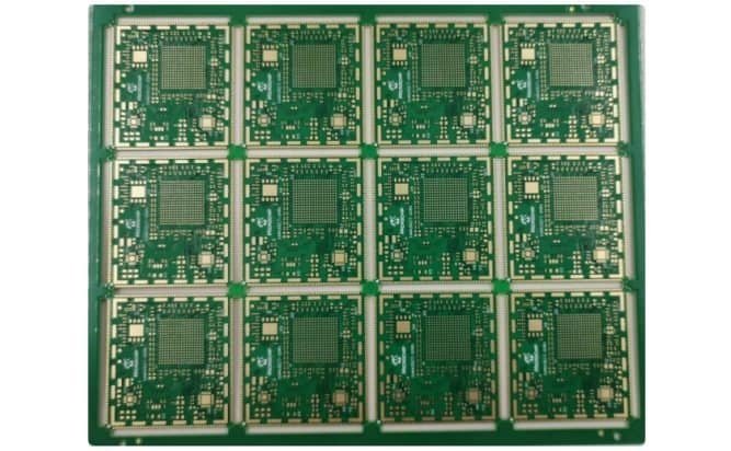
Panelized PCB sample from the PCBSync media library
PCBSync media-library sample illustrating panel format. Project-specific layer count and materials belong in the controlled fabrication record.

What should accompany the quotation?

  • Confirm exactly one intended conductive copper layer.
  • Attach jumper references and mounting instructions.
  • Mark critical current loops and sensitive returns.
  • Specify substrate, hole treatment and finish.

Match the quoted construction, inspection scope and delivery requirements to the released revision. Confirm what is included before placing an order.

Specific questions

single layer PCB questions, answered.

Is a single layer PCB the same as a single-sided PCB?

For the conventional rigid construction discussed here, yes: both describe one conductive copper layer. Mask, legend and substrate do not add to that count. Flexible and metal-backed boards need additional construction details.

Can a single-sided PCB use surface-mount parts?

Yes. SMT pads and components occupy the copper face. Through-hole component bodies may sit on the opposite face. Mixed assembly is possible when placement, soldering access and the assembly process are planned together.

Are jumpers a sign that I need two layers?

A few well-defined jumpers may be practical. Compare alternatives when links consume valuable area, create long critical paths or add substantial assembly work. There is no universal jumper-count threshold.

Can I order one layer by deleting the unused copper Gerber?

Do not rely on file omission alone. State the intended one-copper-layer construction, identify the copper face and verify the exported files. A retained plane or unnoticed pad artwork on the second face changes the requirement.

Will one layer always cost less than two?

No. Board area, quantity, panel utilization, material and assembly operations affect the result. Request like-for-like quotes and include jumpers and their placement cost before selecting a construction.

Engineering quotation

Request a 1-layer PCB review.

Start with the requirements you know. Include unresolved decisions so engineering can review the construction with you.

  • Confirm exactly one intended conductive copper layer.
  • Attach jumper references and mounting instructions.
  • Mark critical current loops and sensitive returns.
  • Specify substrate, hole treatment and finish.
  • Compare the entire assembly with a two-layer option.

Attach fabrication data, the proposed stackup and quantity breaks when ready. For assembly, include the BOM, placement data and inspection requirements.

Discuss NDA arrangements before sharing confidential files. Ask for current certification scope and records relevant to your project.

Contact PCBSync · Include PCB assembly

Drag & Drop Files, Choose Files to Upload You can upload up to 3 files.

Further engineering reading: Würth Elektronik: Basic PCBs Würth Elektronik: BASIC Design Rules

PCBSync engineering resources · Updated 1 October 2026 · Planning guidance and illustrations are not approved manufacturing stackups.