Contact Sales & After-Sales Service

Contact & Quotation

  • Inquire: Call 0086-755-23203480, or reach out via the form below/your sales contact to discuss our design, manufacturing, and assembly capabilities.
  • Quote: Email your PCB files to [email protected] (Preferred for large files) or submit online. We will contact you promptly. Please ensure your email is correct.
One place for your enquiry

Continue on Contact

  1. Download the planning worksheet and review the open items.
  2. Send your requirements and available fabrication files on Contact.
  3. Agree the construction, inspection scope and quotation before ordering.
Request a project review →

Need an NDA or a particular file-transfer method? Contact us before sharing confidential files.

Notes:
For PCB fabrication, we require PCB design file in Gerber RS-274X format (most preferred), *.PCB/DDB (Protel, inform your program version) format or *.BRD (Eagle) format. For PCB assembly, we require PCB design file in above mentioned format, drilling file and BOM. Click to download BOM template To avoid file missing, please include all files into one folder and compress it into .zip or .rar format.

End-to-end channel requirements and named via families

20 Layer PCB: Review the Channel and the Via Family Together

A 20 layer PCB is best specified as a set of electrical paths through a defined construction. A channel uses traces, package escapes, vias and connectors; its behavior cannot be inferred from layer count or laminate name alone. Use a channel matrix and a via-family schedule to connect the routing plan with a reviewable fabrication quotation.

Design decisions · Construction review · Fabrication & assembly planning

20-layer channel-to-via-family mapPlanning illustration: 20-layer channel-to-via-family map. Read the labelled review points below the figure. This is not an approved manufacturing stackup.20 LAYERS / PLANNING CONCEPTThroughTransitionChannelName each family and its span
  • Channel class
  • Routing reference
  • Through family
  • Selected transition
  • Engineering concept

Planning illustration. Geometry and layer roles require project review; no dimensions or process approval are implied.

20-layer channel-to-via-family map. Engineering illustration; the layer count does not establish a qualified manufacturing process.
Define the project

20-Layer Channel and Via-Family Review

Configure the board and prepare your design questions. This custom layer count uses an engineering quotation. The tool prepares a specification and decision brief without inventing a price.

Engineering worksheet · no sign-up

Channel-loss budget

Use loss values at one stated frequency and the same reference planes. Unknown losses remain unknown.

Enable JavaScript to use this worksheet. You can also send your requirements through Contact.

Discuss this project →

Inputs stay in this page until you download them. Nothing is submitted automatically. Review the worksheet, then attach it on Contact.

WORKED ENGINEERING EXAMPLE

Allocate a channel budget without inventing a loss model

Hypothetical design scenario · Original conceptual diagram · Not a customer case or approved fabrication specification

Allocate a channel budget without inventing a loss model. Original conceptual engineering diagram; hypothetical values.Illustrative 12 dB allocation at one frequencyTrace 6 + connector 2 + via 1 + other 1 = 10 dB2 dB remains — not a simulated channel result
Allowed: 12 dB · Allocated: 10 dB · Remaining: 2 dB. Diagram is not to scale.

At one stated evaluation frequency, suppose an allowable insertion-loss budget is 12 dB. An illustrative allocation of 6 dB to traces, 2 dB to connectors, 1 dB to vias and 1 dB to other effects totals 10 dB, leaving 2 dB. These are hypothetical allocations, not predictions for a twenty-layer board.

Use this in your design review

  1. Use consistent frequency, ports and loss definitions for all entries.
  2. Replace assumptions with a suitable channel model or measured data.
  3. Review via families and return transitions separately from the arithmetic.

What to bring to the review

A budget margin does not verify eye opening, return loss or compliance. State what evidence will close each uncertain allocation.

Discuss this construction →
Board specifications, layer concepts & fabrication brief
PCBSync engineering workbench

20 Layer PCB design & cost planner

Plan the board. Compare the construction. Prepare a useful RFQ.

Enable JavaScript for the planner, or use the Contact page. No sign-in or design-file upload is needed to explore the tool.

01 / Your board specification

02 / Electrical structure

Compare the role of each copper layer before committing to a layout. Coloured rows show electrical assignments, not dielectric dimensions or a pressed stackup.

Confirm material grade, copper, dielectric spacing, impedance and tolerance with engineering. Extra layers alone do not guarantee a continuous return path.

Electrical concept

Signal / ground / power · not to scale

Engineering limits and data storage

This tool prepares specifications; it does not inspect files or issue a price, approved stackup, impedance result or delivery commitment. Non-personal specifications may be retained in this browser tab for two hours. Download and review your brief before sending it through Contact.

Define the electrical path

Create one row for each meaningful channel class

Group interfaces that share routing rules and similar physical paths. Record the transmitter and receiver, connector models if present, approximate route length, target data rate or relevant frequency range, and the applicable device or interface guidance. A short device-to-device link should not inherit a long backplane's material choice without analysis.

Assign each group to candidate routing layers and references. Include its escape sections and vertical transitions in the review. If the design has several channel lengths, retain the difficult cases rather than presenting only the shortest example. The purpose is to connect an electrical requirement to a physical route that the fabrication team can identify.

  • Document the operating condition and the model revision used for validation.
  • Keep receiver/equalization assumptions visible when evaluating a channel budget.
Materials with context

Choose the laminate and copper from the loss requirement

Request material data relevant to the analysis frequency and construction. Dielectric constant and dissipation factor values depend on the measurement method and frequency; a single marketing number is not a complete model. Include copper foil and surface treatment assumptions when the channel analysis is sensitive to conductor loss.

Compare a uniform material construction with a mixed-material option only when the supplier can review the whole build. Identify exactly which dielectric intervals serve the critical paths and what remains unchanged elsewhere. A hybrid stack can introduce procurement and processing differences, so ask for the proposed material list and approval process. Do not convert a material family into a guaranteed channel speed or a fixed cost multiplier.

20-Layer Channel and Via-Family Review

  1. Channel definition
  2. Material proposal
  3. Via documentation
  4. Planned electrical evidence
  5. Unused via barrel review

Work through these decisions in the planner. Keep the resulting brief attached to the same project revision.

A review sequence for this 20-layer project. Selections in the tool create your own brief.
Vertical interconnect schedule

Give each distinct transition a stable identity

Create a via family whenever the construction, layer span or electrical purpose changes. A full through hole, a selected backdrilled transition and a buried interconnect should not share one ambiguous note. Record the connected layers, pad and antipad geometry, reference-via arrangement where relevant, and any fill or cap requirements.

Map the channel classes to those families. This exposes a common late-stage problem: a route changes layer and silently acquires a different transition than the one analyzed. Keep the family names consistent between layout rules, fabrication drawings and simulation notes. The supplier can then review each structure against the proposed thickness and process sequence.

Family fieldDesign questionFabrication handoff
Connected layersWhere does the signal enter and exit?Named copper layers
Hole constructionThrough, blind, buried or backdrilled?Drill/process schedule
Surrounding copperWhat pads, antipads and returns exist?Reviewed dimensions
VerificationWhat evidence does this structure need?Model, coupon or inspection requirement
Verification scope

Separate trace impedance, transition behavior and full-channel results

A coupon specified for PCB impedance control can check the characteristic impedance of a representative trace construction. It does not automatically validate a connector launch, every via transition or the complete channel. Decide which structures need electromagnetic analysis and whether prototype measurements are needed for the performance objective.

When a residual via barrel is significant, set its requirement through the channel review and confirm what the process can achieve. Include tolerance extremes rather than evaluating only nominal geometry. Agree the coupon design, measurement method and reporting scope before tooling if those reports are part of acceptance. A continuity test and a channel measurement answer different questions.

  • Match any measured coupon to the construction and revision being supplied.
  • Retain the assumptions needed to reproduce the electrical comparison.
Engineering quotation

Purchase the reviewed construction with controlled alternatives

Send the channel matrix, via-family schedule, proposed stack, outline and fabrication data together. State the quantity, lot strategy, required reports and the material alternatives that may be considered. Ask the supplier to list engineering exceptions and any changes to the proposed family geometries.

Confirm which records accompany the prototype and which continue into repeat production. A quotation should identify the materials and fabrication operations it includes, such as selected backdrilling or sequential build steps if required. Twenty layers alone does not prescribe those operations. Approval of the complete engineering proposal gives procurement a defined scope for price and schedule comparison.

  • Tie the quote to a stack and drawing revision.
  • Require review before a material, hole span or controlled geometry is substituted.
From requirements to evidence

Connect the proposed construction to the inspection plan.

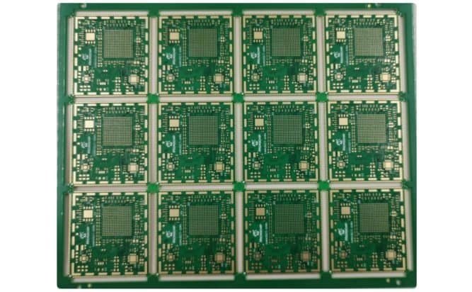
Panelized PCB sample from the PCBSync media library
PCBSync media-library sample illustrating panel format. Project-specific layer count and materials belong in the controlled fabrication record.

What should accompany the quotation?

  • Each channel class has an identifiable physical route.
  • Each transition references a named via family.
  • Material data matches the intended model.
  • The quotation lists the required verification records.

Match the quoted construction, inspection scope and delivery requirements to the released revision. Confirm what is included before placing an order.

Specific questions

20 Layer PCB questions, answered.

Does a 20 layer PCB automatically support a particular data rate?

No. Channel length, geometry, materials, transitions, connectors and device capabilities determine performance. Layer count provides routing resources but is not an electrical performance rating.

Is a low-loss material necessary on every dielectric interval?

That depends on the paths and the fabricator's available constructions. Evaluate the critical channels first, then review any mixed-material proposal for electrical and processing compatibility.

What is a via family?

It is a named group of vias sharing a defined span and construction. Separate families allow layout, fabrication and validation teams to reference the same geometry without relying on one generic via note.

Does an impedance report prove the full channel passes?

No. Trace impedance is one part of channel behavior. Via transitions, connectors, route length and loss still require the appropriate analysis or measurements for the interface.

How is a 20 layer PCB priced?

Use an engineering quotation based on the actual materials, size, thickness, hole construction, quantity and acceptance scope. An automatic layer multiplier cannot account for these process and verification differences.

Engineering quotation

Request a 20-layer PCB review.

Start with the requirements you know. Include unresolved decisions so engineering can review the construction with you.

  • Each channel class has an identifiable physical route.
  • Each transition references a named via family.
  • Material data matches the intended model.
  • The quotation lists the required verification records.

Attach fabrication data, the proposed stackup and quantity breaks when ready. For assembly, include the BOM, placement data and inspection requirements.

Discuss NDA arrangements before sharing confidential files. Ask for current certification scope and records relevant to your project.

Contact PCBSync · Include PCB assembly

One place for your enquiry

Continue on Contact

  1. Download the planning worksheet and review the open items.
  2. Send your requirements and available fabrication files on Contact.
  3. Agree the construction, inspection scope and quotation before ordering.
Request a project review →

Need an NDA or a particular file-transfer method? Contact us before sharing confidential files.

PCBSync engineering resources · Updated 1 October 2026 · Planning guidance and illustrations are not approved manufacturing stackups.