Contact Sales & After-Sales Service

Contact & Quotation

  • Inquire: Call 0086-755-23203480, or reach out via the form below/your sales contact to discuss our design, manufacturing, and assembly capabilities.
  • Quote: Email your PCB files to [email protected] (Preferred for large files) or submit online. We will contact you promptly. Please ensure your email is correct.
Drag & Drop Files, Choose Files to Upload You can upload up to 3 files.

Notes:
For PCB fabrication, we require PCB design file in Gerber RS-274X format (most preferred), *.PCB/DDB (Protel, inform your program version) format or *.BRD (Eagle) format. For PCB assembly, we require PCB design file in above mentioned format, drilling file and BOM. Click to download BOM template To avoid file missing, please include all files into one folder and compress it into .zip or .rar format.

PCBSync · RF materials & PCB manufacturing

PTFE PCB Material: Reinforcement, Dk & Design Choices

Choose a PTFE laminate by its actual construction and data. Understand what glass reinforcement, ceramic filler, foil and dielectric thickness change before specifying an RF board.

Stack-up, test scope, price and schedule confirmed after file review.

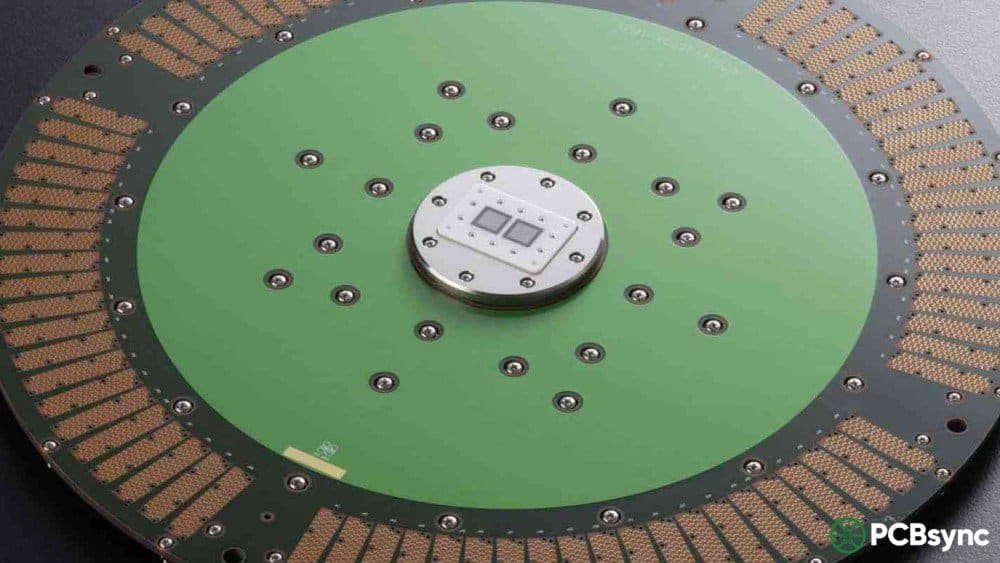
Physical PCB sample with repeated meandering conductors and plated connection pads. Confirm the exact laminate and RF response from project records.

Key distinction: PTFE names the polymer; a PCB laminate is a composite. The polymer name alone cannot specify electrical behavior, stiffness or a manufacturing process.

Explore the design before release

PTFE PCB Material tools & quotation planning

PTFE PCB Material project tools

PCBSync Engineering Tools · calculations run in your browser · no account required

Compare entered Dk and Df readings. Example A/B values are illustrative, not named-material presets. A delta is issued only when frequency, method and specimen basis match; the reports still need review.

Candidate A

Candidate B

Start with your design inputs

Example values are editable. Review the result and assumptions before adding a scenario to your enquiry.

Design tips and manufacturing decisions

PTFE PCB Material: what to resolve before fabrication

Resin is only one part of the laminate

PTFE PCB materials combine a fluoropolymer with a particular reinforcement and, in some grades, filler. Reinforcement influences handling and dimensional behavior; filler changes the composite response. A sheet of generic PTFE and a reinforced copper-clad RF laminate are not interchangeable procurement items.

Start the drawing with a manufacturer and complete product designation. Add dielectric thickness, copper type and permitted tolerance. If purchasing is allowed to suggest equivalents, define who approves the electrical and mechanical comparison. For Taconic PCB material selection, apply the same checks to the complete quoted grade rather than to the brand name alone.

Read Dk and Df as measurements with conditions

Record the frequency, test method and specimen basis beside the value. A clamped-stripline result, a resonator result and a design Dk fitted to a particular circuit may serve different purposes. A low loss tangent is not the same as low total transmission-line insertion loss.

The comparison tool checks the conditions you enter before displaying an arithmetic difference. It cannot verify the test reports. Matching labels still require a review of conditioning, material direction, thickness and procedure revision.

Understand what a thin core changes

For a given routing structure, the trace-to-plane spacing affects the width needed for a target impedance. A thinner core can require finer geometry and make conductor thickness, etch shape and manufacturing variation more significant. Total board thickness is not the local dielectric gap.

Identify the controlled layer and its reference plane. Use the early line calculator only for the structures it supports; ask for a suitable model when coplanar ground, solder mask or an asymmetric stack-up changes the field distribution.

Copper foil and finish belong in the RF specification

Copper profile and surface treatment are part of the physical interconnect. Ask which foil and finish are proposed, especially where the loss or phase budget is tight. The laminate datasheet does not account for every finished conductor or launch in your design.

Keep comparisons at a common frequency and reference plane. If a measured attenuation number already includes connectors, do not add the same launch allowance again when evaluating the route.

Release a material system, not a generic family

A multilayer board needs a compatible core and bond-layer system, processed to a qualified construction. Material dimensional change, via preparation and final thickness must be reviewed together. Avoid importing generic FR-4 fabrication assumptions into an unfamiliar PTFE stack-up.

The RFQ should identify open material choices and request a proposed construction. Confirm the selected material, copper and test scope before authorizing a change to the fabrication drawing.

A clearer brief gets a clearer response

Four requirements for this enquiry

01

Full laminate designation and reinforcement

02

Dk / Df frequency, method and specimen basis

03

Dielectric spacing, copper and finish

04

Bonding system and acceptance evidence

Attach the current fabrication files and drawing revision. Mark open questions, permitted alternatives and requested delivery timing. For assembly, add BOM and placement files. Ask for exceptions and additional test costs to be identified in the response.

Real physical circuits

Physical PCB examples and construction details

These photographs show visible conductor patterns, pads and mechanical features. Confirm material identity, electrical performance and application qualification through approved project records.

Answers for design and procurement

PTFE PCB Material FAQ

Is every Rogers material PTFE?

No. A brand includes different resin systems. Check the named product rather than treating a brand as a polymer.

Is lower Dk always better?

No. It affects geometry and field distribution. Circuit size, impedance, loss, thermal behavior and manufacturability must be considered together.

How do I request an engineering quotation?

Prepare current fabrication files, the proposed stack-up, quantity and requested delivery. Include material and inspection requirements. For controlled-impedance work, add target impedance, signal mode, controlled layers, reference planes and permitted geometry changes. Mark open questions for review. The planner is optional; you can request a quote with the information you have.

References checked 2 October 2026. Historical sources are labeled. Calculations are planning aids. Use current interface requirements, construction-specific models and agreed test procedures for design release.

From requirements to a reviewable quotation

Discuss your PTFE PCB Material project

Send the construction you want reviewed

If useful, add a planning result and your assumptions to the enquiry. Include the board revision, quantity, requested arrival date and open questions. Ask the quotation to identify the proposed stack-up, exceptions and inspection scope.

Need an NDA or a particular file-transfer arrangement? Contact us before sending files.

Email: [email protected]
Phone: +86-755-23203480

Review your message and attachments before submitting. An enquiry does not place an order.

Drag & Drop Files, Choose Files to Upload You can upload up to 3 files.