Contact Sales & After-Sales Service

Contact & Quotation

  • Inquire: Call 0086-755-23203480, or reach out via the form below/your sales contact to discuss our design, manufacturing, and assembly capabilities.
  • Quote: Email your PCB files to [email protected] (Preferred for large files) or submit online. We will contact you promptly. Please ensure your email is correct.
One place for your enquiry

Continue on Contact

  1. Download the planning worksheet and review the open items.
  2. Send your requirements and available fabrication files on Contact.
  3. Agree the construction, inspection scope and quotation before ordering.
Request a project review →

Need an NDA or a particular file-transfer method? Contact us before sharing confidential files.

Notes:
For PCB fabrication, we require PCB design file in Gerber RS-274X format (most preferred), *.PCB/DDB (Protel, inform your program version) format or *.BRD (Eagle) format. For PCB assembly, we require PCB design file in above mentioned format, drilling file and BOM. Click to download BOM template To avoid file missing, please include all files into one folder and compress it into .zip or .rar format.

Twelve-layer routing resources and conventional versus HDI manufacturing

12 Layer PCB: Separate Layer Count from HDI

Twelve copper layers can give a dense design more routing and reference resources. They do not automatically require microvias, backdrilling or a particular laminate. Determine the escape geometry and channel needs first, then compare conventional and advanced interconnect constructions.

Design decisions · Construction review · Fabrication & assembly planning

Same copper count, different interconnect choicesPlanning illustration: Same copper count, different interconnect choices. Read the labelled review points below the figure. This is not an approved manufacturing stackup.12 LAYERS / PLANNING CONCEPTThrough holeHDI option12 copper levels in each concept
  • 12 copper layers
  • Conventional through-hole option
  • Package escape constraint
  • Via family and buildup need approval

Planning illustration. Geometry and layer roles require project review; no dimensions or process approval are implied.

Same copper count, different interconnect choices. Engineering illustration; the layer count does not establish a qualified manufacturing process.
Define the project

Twelve-layer through-hole or HDI decision

Configure the board and prepare your design questions. A rigid FR-4 reference base budget is available for supported scenarios; other materials and custom processes need separate quotation.

Engineering worksheet · no sign-up

BGA escape feasibility worksheet

Pitch alone cannot establish the need for HDI. Review populated rows, pad geometry and the agreed process together.

Enable JavaScript to use this worksheet. You can also send your requirements through Contact.

Discuss this project →

Inputs stay in this page until you download them. Nothing is submitted automatically. Review the worksheet, then attach it on Contact.

WORKED ENGINEERING EXAMPLE

Check the escape channel before choosing HDI

Hypothetical design scenario · Original conceptual diagram · Not a customer case or approved fabrication specification

Check the escape channel before choosing HDI. Original conceptual engineering diagram; hypothetical values.0.80 mm center spacing0.10 mm trace + 2 × 0.10 mm spaceSimplified geometry — verify actual escape rules
Gap: 0.40 mm · Trace + spaces: 0.30 mm · Nominal remainder: 0.10 mm. Diagram is not to scale.

For an illustrative 0.80 mm pad-center spacing and 0.40 mm pad diameter, the nominal gap is 0.40 mm. A 0.10 mm trace with 0.10 mm clearance on each side occupies 0.30 mm. This leaves 0.10 mm in the simplified drawing, but ignores tolerances, via lands, mask and local routing restrictions; it is not a routing approval.

Use this in your design review

  1. Use the actual pad, via-land and clearance geometry.
  2. Check how signals reach every intended routing layer.
  3. Compare conventional drilling and HDI only after identifying the real bottleneck.

What to bring to the review

Supply the package drawing, pad geometry and escape constraints. Pitch alone cannot determine the required via process or layer count.

Discuss this construction →
Board specifications, layer concepts & fabrication brief
PCBSync engineering workbench

12 Layer PCB design & cost planner

Plan the board. Compare the construction. Prepare a useful RFQ.

Enable JavaScript for the planner, or use the Contact page. No sign-in or design-file upload is needed to explore the tool.

01 / Your board specification

02 / Electrical structure

Compare the role of each copper layer before committing to a layout. Coloured rows show electrical assignments, not dielectric dimensions or a pressed stackup.

Confirm material grade, copper, dielectric spacing, impedance and tolerance with engineering. Extra layers alone do not guarantee a continuous return path.

Electrical concept

Signal / ground / power · not to scale

Engineering limits and data storage

This tool prepares specifications; it does not inspect files or issue a price, approved stackup, impedance result or delivery commitment. Non-personal specifications may be retained in this browser tab for two hours. Download and review your brief before sending it through Contact.

Layer planning

Reserve references before estimating routing capacity

Begin with package escape, net classes, power domains and the allowed board outline. A twelve-layer layout may use six signal layers and six plane layers, but other allocations can be valid. What matters is whether the available routing corridors remain useful after reference planes, via antipads, connector fields and keepouts are included.

One conceptual six-signal allocation is S–G–S–G–S–P–P–S–G–S–G–S. It places ground adjacent to each signal level while reserving two power levels. This is a functional example, not a released production construction. Actual material spacing, coupling, copper coverage and distribution requirements still determine whether the arrangement suits the design.

  • Map each critical signal class to its routing and reference levels.
  • Check power-plane necks and clearances after via placement.
  • Keep the layer budget tied to the actual component and connector arrangement.
BGA escape

Test the package geometry before choosing the via technology

BGA pitch alone does not determine whether a twelve-layer board needs HDI. The ball map, pad size, allowed trace/space, via pad, antipad and unused pin pattern all affect escape. A package with accessible routing corridors can differ substantially from another at the same pitch. Perform an escape trial using geometry the proposed fabricator can actually support.

Start with a conventional through-hole option where feasible and identify the precise obstacle. Is a via pad blocking another channel, does an antipad remove too much reference copper, or do the inner rows lack access? That evidence lets you compare smaller interconnects, a changed pin assignment, more routing resources or a different package. It also prevents advanced processes being specified without a defined benefit.

  • Use the component vendor's land pattern and routing guidance.
  • Show the escape trial and unresolved rows in the review package.
  • Separate local escape congestion from long-distance channel requirements.

Twelve-layer through-hole or HDI decision

  1. Package escape evidence
  2. Proposed interconnect family
  3. Critical via-stub assessment
  4. Routing and reference budget
  5. Release evidence planned

Work through these decisions in the planner. Keep the resulting brief attached to the same project revision.

A review sequence for this 12-layer project. Selections in the tool create your own brief.
Manufacturing paths

Through-holes, HDI and backdrilling solve different problems

A conventional twelve-layer board can use plated through-holes connecting selected copper levels. HDI structures may add laser-drilled microvias and sequential buildup to access dense regions without sending every interconnect through the full board. Buried vias, blind vias and filled via-in-pad features each require a defined structure and process. The words twelve layers do not specify any of these features.

Backdrilling addresses unwanted plated barrel sections on suitable through-vias. It does not replace fine-pitch escape technology, and microvias do not eliminate the need to review the remaining channel transitions. Describe every via family by start/end layers, hole or cavity requirement, filling/capping needs and electrical purpose. Ask the fabricator to review the complete buildup rather than approving independent via names.

ChoicePrimary design questionInformation to provide
Plated through-holeCan pads and clearances fit the escape?Finished hole, pads, antipads and connected layers
Blind/buried or microviaWhich specific connections need shorter access?Via spans and complete buildup sequence
Via-in-padDoes the component pad need an interconnect beneath it?Fill/cap and assembly pad requirements
BackdrillDoes a through-via stub exceed channel needs?Entry side, stop region, clearance and remnant target
Construction

Coordinate thickness, material and controlled geometry

The mechanical board thickness must fit the product while leaving a manufacturable copper-and-dielectric structure. For a proposed thickness, review core and bonding material availability, drilled-hole geometry and copper requirements together. More layers at the same thickness usually redistribute the available dielectric space; they do not preserve the geometry of a lower-layer design.

Set PCB impedance control targets by net class and identify which layers will carry them. Material selection should follow loss, thermal and processing requirements, with approved substitutions stated clearly. Do not equate high-Tg PCB material with low loss or assume that all FR-4 grades share one dielectric constant. Hybrid materials need review as a complete construction, including compatibility and mechanical balance.

  • Define nominal thickness and tolerance for mechanical interfaces.
  • State copper requirements consistently as foil or finished copper.
  • Freeze the accepted impedance geometries after the material construction is agreed.
Release evidence

Choose the production path with a verifiable file set

Compare a twelve-layer through-hole design with an HDI version using the same required function and acceptance criteria. Include the effect on board area, routing completion, lamination requirements, inspection and assembly. A lower layer count with advanced vias is not automatically cheaper, and adding layers does not always solve package escape. If twelve remains constrained, identify the useful resources that fourteen would add.

Release a coherent package: layer order, material construction, copper files, drill-family drawing, impedance table and any backdrill notes. Specify the evidence needed for the project, such as electrical-test results, relevant impedance coupons or agreed microsection inspection. A sample coupon checks defined features under agreed conditions; it does not prove that every high-speed channel meets the system specification.

  • Keep construction and via-family revisions synchronized.
  • Record acceptance requirements before comparing quotes.
  • Use engineering pricing for advanced interconnects or materials outside the reference model.
From requirements to evidence

Connect the proposed construction to the inspection plan.

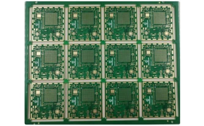
Panelized PCB sample from the PCBSync media library
PCBSync media-library sample illustrating panel format. Project-specific layer count and materials belong in the controlled fabrication record.

What should accompany the quotation?

  • Complete a realistic package escape trial.
  • Separate layer count from HDI and backdrill choices.
  • Define every via family and material region.
  • Map critical nets to continuous references.

Match the quoted construction, inspection scope and delivery requirements to the released revision. Confirm what is included before placing an order.

Specific questions

12 layer PCB questions, answered.

Is a twelve-layer PCB automatically an HDI PCB?

No. Twelve describes the conductive copper count. HDI describes additional interconnect and density choices. A twelve-layer board may use conventional through-holes when the geometry and electrical requirements permit.

How many signal layers should a twelve-layer board have?

There is no fixed number. Six is one possible allocation, but routing demand, references and power distribution may justify another. Verify usable channels after escape and plane clearances are included.

Does every twelve-layer PCB need backdrilling?

No. Evaluate the actual via stub and channel requirements. Backdrilling is a defined optional process with geometric constraints, not an automatic consequence of having twelve layers.

Can more layers eliminate the need for microvias?

Sometimes additional routing resources help, but they cannot necessarily overcome a local pad or via-clearance blockage. Compare an actual package escape trial with the proposed interconnect geometries.

What makes a twelve-layer quote ready for approval?

An agreed material stackup, complete layer order, via-family definition, impedance requirements, mechanical tolerances and acceptance plan. The price should identify optional advanced processes and the exact construction revision.

Engineering quotation

Request a 12-layer PCB review.

Start with the requirements you know. Include unresolved decisions so engineering can review the construction with you.

  • Complete a realistic package escape trial.
  • Separate layer count from HDI and backdrill choices.
  • Define every via family and material region.
  • Map critical nets to continuous references.
  • Release one synchronized construction and acceptance package.

Attach fabrication data, the proposed stackup and quantity breaks when ready. For assembly, include the BOM, placement data and inspection requirements.

Discuss NDA arrangements before sharing confidential files. Ask for current certification scope and records relevant to your project.

Contact PCBSync · Include PCB assembly

One place for your enquiry

Continue on Contact

  1. Download the planning worksheet and review the open items.
  2. Send your requirements and available fabrication files on Contact.
  3. Agree the construction, inspection scope and quotation before ordering.
Request a project review →

Need an NDA or a particular file-transfer method? Contact us before sharing confidential files.

PCBSync engineering resources · Updated 1 October 2026 · Planning guidance and illustrations are not approved manufacturing stackups.