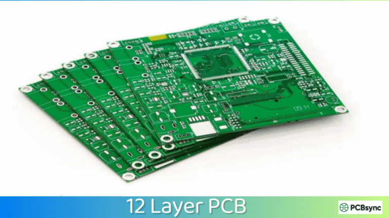
Contact Sales & After-Sales Service

Contact & Quotation

  • Inquire: Call 0086-755-23203480, or reach out via the form below/your sales contact to discuss our design, manufacturing, and assembly capabilities.
  • Quote: Email your PCB files to [email protected] (Preferred for large files) or submit online. We will contact you promptly. Please ensure your email is correct.
One place for your enquiry

Continue on Contact

  1. Download the planning worksheet and review the open items.
  2. Send your requirements and available fabrication files on Contact.
  3. Agree the construction, inspection scope and quotation before ordering.
Request a project review →

Need an NDA or a particular file-transfer method? Contact us before sharing confidential files.

Notes:
For PCB fabrication, we require PCB design file in Gerber RS-274X format (most preferred), *.PCB/DDB (Protel, inform your program version) format or *.BRD (Eagle) format. For PCB assembly, we require PCB design file in above mentioned format, drilling file and BOM. Click to download BOM template To avoid file missing, please include all files into one folder and compress it into .zip or .rar format.

Value of the two additional copper layers when moving from 12 to 14

14 Layer PCB: Make the Two Added Layers Count

A 14 layer PCB has fourteen copper layers, but the useful gain over a twelve-layer design depends on how those layers are assigned. Start with the routing bottleneck: crowded escape channels, missing reference planes, power distribution, or excessive detours. Use this review to turn that problem into a layer allocation and a project-specific engineering quotation.

Design decisions · Construction review · Fabrication & assembly planning

14-layer resource allocation conceptPlanning illustration: 14-layer resource allocation concept. Read the labelled review points below the figure. This is not an approved manufacturing stackup.14 LAYERS / PLANNING CONCEPT12 → 14Signal accessReference pathPower resource
  • 14 copper layers
  • Added resource pair
  • Signal access
  • Reference continuity

Planning illustration. Geometry and layer roles require project review; no dimensions or process approval are implied.

14-layer resource allocation concept. Engineering illustration; the layer count does not establish a qualified manufacturing process.
Define the project

14-Layer Resource Review

Configure the board and prepare your design questions. This custom layer count uses an engineering quotation. The tool prepares a specification and decision brief without inventing a price.

Engineering worksheet · no sign-up

12 / 14 / 16-layer comparison

Keep material, dimensions, copper, via and inspection assumptions comparable. Identify the routing resource actually added by each option.

Enable JavaScript to use this worksheet. You can also send your requirements through Contact.

Discuss this project →

Inputs stay in this page until you download them. Nothing is submitted automatically. Review the worksheet, then attach it on Contact.

WORKED ENGINEERING EXAMPLE

Show what the additional layer pair resolves

Hypothetical design scenario · Original conceptual diagram · Not a customer case or approved fabrication specification

Show what the additional layer pair resolves. Original conceptual engineering diagram; hypothetical values.0112: two open issues0214: named resources0316: alternative review
12: two open issues · 14: named resources · 16: alternative review. Diagram is not to scale.

A hypothetical twelve-layer design has one unresolved interface route and insufficient reference continuity in that region. The fourteen-layer proposal should identify which additional routing or plane resource fixes each issue. If both issues remain, the layer-count increase has not demonstrated value.

Use this in your design review

  1. Record the specific limitations of the twelve-layer baseline.
  2. Assign a measurable purpose to each added copper layer.
  3. Recheck thickness, via access and impedance after the change.

What to bring to the review

Keep the comparison on a common outline, quantity, material scope and inspection requirement. This makes the engineering and quotation differences reviewable.

Discuss this construction →
Board specifications, layer concepts & fabrication brief
PCBSync engineering workbench

14 Layer PCB design & cost planner

Plan the board. Compare the construction. Prepare a useful RFQ.

Enable JavaScript for the planner, or use the Contact page. No sign-in or design-file upload is needed to explore the tool.

01 / Your board specification

02 / Electrical structure

Compare the role of each copper layer before committing to a layout. Coloured rows show electrical assignments, not dielectric dimensions or a pressed stackup.

Confirm material grade, copper, dielectric spacing, impedance and tolerance with engineering. Extra layers alone do not guarantee a continuous return path.

Electrical concept

Signal / ground / power · not to scale

Engineering limits and data storage

This tool prepares specifications; it does not inspect files or issue a price, approved stackup, impedance result or delivery commitment. Non-personal specifications may be retained in this browser tab for two hours. Download and review your brief before sending it through Contact.

Start with the obstruction

Record what the twelve-layer version cannot route

Mark the congested region and the affected net classes before changing the stack. A package escape can be blocked by pad and via geometry even when open routing area remains elsewhere. A long interface may instead need another continuous corridor between endpoints. Those are different problems, and another signal layer only helps when the nets can reach and use it.

Keep a short before-and-after record: unrouted nets, longest detour, layer changes and the reference assigned to each route. If the obstruction is local, compare component rotation, legal pin swaps and a revised via pattern as well. Fourteen layers becomes a defensible choice when the allocation addresses the documented constraint.

  • Name the package or route corridor that needs capacity.
  • Identify whether the missing resource is copper area, a reference, or access through the via field.
Allocate before drawing

Two additional copper layers do not always mean two signal layers

A revised allocation might add routing capacity, restore a reference plane that was being used for signals, or give a power domain a more practical distribution layer. Decide the electrical roles first, then ask the fabricator to arrange cores and prepregs around them. A resource tally is an accounting tool; it does not establish the final layer order.

Check each critical signal layer against its intended reference and every transition against the return-current path. Reserving another ground plane can make an existing signal layer more useful. Conversely, adding routing between poorly chosen references may increase nominal capacity without producing a route that meets the interface rules.

14-Layer Resource Review

  1. Primary bottleneck
  2. Intended use of added resources
  3. Overall thickness constraint
  4. Twelve-layer baseline

Work through these decisions in the planner. Keep the resulting brief attached to the same project revision.

A review sequence for this 14-layer project. Selections in the tool create your own brief.
Reason to add layersResource to evaluateEvidence to retain
Congested routesUsable signal corridorRoute length and transition comparison
Reference discontinuityContinuous reference planeReference map through the full route
Power distributionPlane area and interconnectionsCurrent-path and voltage-drop review
Keep the whole board in view

Reconcile the allocation with thickness and drilling

Freeze the connector and enclosure constraints before selecting the new dielectric gaps. If overall thickness is fixed, adding copper and dielectric interfaces redistributes the available thickness; it does not simply create two free routing surfaces. A revised gap changes the trace geometry used for PCB impedance control and can affect how traces escape a package.

Review the smallest mechanically drilled hole against the proposed board thickness using the supplier's stated diameter convention. Keep drill-tool diameter and finished plated-hole diameter separate. Also check connector pin engagement, press-fit requirements where applicable, mounting hardware and assembly support. The resource gain is useful only when the electrical and mechanical designs remain compatible.

  • Obtain a proposed pressed stack from the intended fabrication process.
  • Recheck impedance geometry and via clearances after thickness changes.
Review the layout as well as the stack

Preserve a workable copper distribution

A symmetric-looking layer list does not show whether the finished copper patterns are balanced. Compare copper thicknesses across the mid-plane and review where dense plane areas face sparse routing. Keep the fabricator involved when copper fill or panel balancing is proposed; changes inside the circuit can affect spacing, capacitance and sensitive nodes.

Do not impose an arbitrary coverage percentage merely because the board has fourteen layers. Ask for an analysis appropriate to the actual dimensions, materials and copper pattern. If a special asymmetric construction is necessary, document the reason and request a process review instead of assuming that any asymmetry must fail.

Buy a defined outcome

Request comparable twelve- and fourteen-layer proposals

Send both options with the same outline, quantities, finish, acceptance requirements and delivery destination. Ask each quotation to state the proposed stack revision, material grade, hole families, impedance scope and separately priced tooling or test work. A price based only on the layer number hides the process differences that matter.

Mark which requirements are fixed and which may change. For example, permit a thickness adjustment only if the enclosure allows it, and request approval before substituting the laminate or changing a via structure. Choose between the proposals using routing closure, validation work and the complete build scope. A fourteen-layer price should not be calculated by multiplying a twelve-layer estimate by 14/12.

  • Attach the congestion evidence and the proposed resource allocation.
  • Resolve engineering exceptions before the purchase order identifies a build revision.
From requirements to evidence

Connect the proposed construction to the inspection plan.

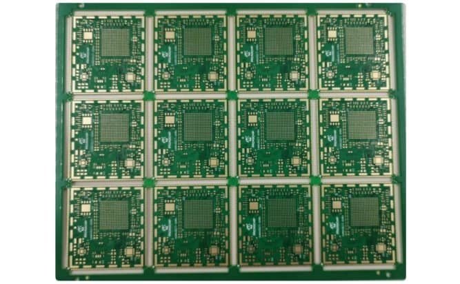
Panelized PCB sample from the PCBSync media library
PCBSync media-library sample illustrating panel format. Project-specific layer count and materials belong in the controlled fabrication record.

What should accompany the quotation?

  • A named bottleneck explains the change.
  • All fourteen copper layers have defined roles.
  • Critical routes retain an intended reference.
  • The supplier has reviewed the revised thickness and hole geometry.

Match the quoted construction, inspection scope and delivery requirements to the released revision. Confirm what is included before placing an order.

Specific questions

14 Layer PCB questions, answered.

Does a 14 layer PCB contain fourteen signal layers?

No. Fourteen is the copper-layer count. Some layers may carry signals, ground, power or mixed regions. Count the roles separately and verify that the signal layers are usable with the required references and escape geometry.

Should the added layers both be ground planes?

Only if that allocation solves the design constraint. Compare the affected net classes, return paths and power requirements. The final physical placement also needs a materials and lamination review.

Can a 14 layer PCB keep the same thickness as a 12 layer board?

It may be possible, depending on copper, dielectric options and fabrication limits. Request a proposed pressed build and revised impedance dimensions; keeping the nominal outline thickness does not preserve all internal geometry.

Is HDI required at fourteen layers?

No. HDI is a choice of interconnect construction, not a consequence of the copper-layer count. Decide from package escape, hole access and electrical requirements, then confirm the complete process with the supplier.

What should accompany a 14 layer PCB quote request?

Include fabrication data, outline, layer roles, thickness limits, materials or allowable alternatives, drill information, controlled nets, quantity and inspection requirements. Explain the change from twelve layers so alternatives can address the same constraint.

Engineering quotation

Request a 14-layer PCB review.

Start with the requirements you know. Include unresolved decisions so engineering can review the construction with you.

  • A named bottleneck explains the change.
  • All fourteen copper layers have defined roles.
  • Critical routes retain an intended reference.
  • The supplier has reviewed the revised thickness and hole geometry.

Attach fabrication data, the proposed stackup and quantity breaks when ready. For assembly, include the BOM, placement data and inspection requirements.

Discuss NDA arrangements before sharing confidential files. Ask for current certification scope and records relevant to your project.

Contact PCBSync · Include PCB assembly

One place for your enquiry

Continue on Contact

  1. Download the planning worksheet and review the open items.
  2. Send your requirements and available fabrication files on Contact.
  3. Agree the construction, inspection scope and quotation before ordering.
Request a project review →

Need an NDA or a particular file-transfer method? Contact us before sharing confidential files.

PCBSync engineering resources · Updated 1 October 2026 · Planning guidance and illustrations are not approved manufacturing stackups.