Contact Sales & After-Sales Service

Contact & Quotation

  • Inquire: Call 0086-755-23203480, or reach out via the form below/your sales contact to discuss our design, manufacturing, and assembly capabilities.
  • Quote: Email your PCB files to [email protected] (Preferred for large files) or submit online. We will contact you promptly. Please ensure your email is correct.
One place for your enquiry

Continue on Contact

  1. Download the planning worksheet and review the open items.
  2. Send your requirements and available fabrication files on Contact.
  3. Agree the construction, inspection scope and quotation before ordering.
Request a project review →

Need an NDA or a particular file-transfer method? Contact us before sharing confidential files.

Notes:
For PCB fabrication, we require PCB design file in Gerber RS-274X format (most preferred), *.PCB/DDB (Protel, inform your program version) format or *.BRD (Eagle) format. For PCB assembly, we require PCB design file in above mentioned format, drilling file and BOM. Click to download BOM template To avoid file missing, please include all files into one folder and compress it into .zip or .rar format.

Total thickness accounting and drill-depth/diameter definitions

18 Layer PCB: Reconcile Thickness, Dielectrics and Drilling

An 18 layer PCB adds copper and dielectric interfaces to the mechanical envelope of the product. The design review should connect that thickness budget to drilled-hole geometry, controlled impedance and connector requirements. Use the steps below to compare a proposed eighteen-layer construction with a sixteen- or twenty-layer alternative before requesting an engineering quotation.

Design decisions · Construction review · Fabrication & assembly planning

18-layer thickness and hole-basis diagramPlanning illustration: 18-layer thickness and hole-basis diagram. Read the labelled review points below the figure. This is not an approved manufacturing stackup.18 LAYERS / PLANNING CONCEPT18 copper / 17 gapsTotalSpanTool Ø ≠ finished hole Ø
  • 18 copper layers
  • 17 dielectric intervals
  • Pressed dielectric
  • Drilled depth
  • Tool diameter / finished hole
  • Geometry only

Planning illustration. Geometry and layer roles require project review; no dimensions or process approval are implied.

18-layer thickness and hole-basis diagram. Engineering illustration; the layer count does not establish a qualified manufacturing process.
Define the project

18-Layer Thickness and Drill Review

Configure the board and prepare your design questions. This custom layer count uses an engineering quotation. The tool prepares a specification and decision brief without inventing a price.

Engineering worksheet · no sign-up

18-layer thickness ledger

Use dielectric-only pressed values and finished copper. Do not count core copper twice.

Enable JavaScript to use this worksheet. You can also send your requirements through Contact.

Discuss this project →

Inputs stay in this page until you download them. Nothing is submitted automatically. Review the worksheet, then attach it on Contact.

WORKED ENGINEERING EXAMPLE

Separate copper thickness from dielectric thickness

Hypothetical design scenario · Original conceptual diagram · Not a customer case or approved fabrication specification

Separate copper thickness from dielectric thickness. Original conceptual engineering diagram; hypothetical values.Copper0.630 mmPressed dielectric only2.040 mmNominal subtotal = 2.670 mmOuter allowances and tolerances require review
Copper: 0.630 mm · Dielectric: 2.040 mm · Subtotal: 2.670 mm. Diagram is not to scale.

Illustratively, eighteen copper layers at 35 micrometres total 0.630 mm. If seventeen dielectric-only pressed intervals average 0.120 mm, they total 2.040 mm. Their sum is 2.670 mm before any separately counted outer coating or finish allowance. Real constructions use actual interval values, not this uniform average.

Use this in your design review

  1. Enter finished copper consistently for every layer.
  2. Use dielectric-only pressed intervals to avoid double counting.
  3. Confirm which thickness basis and hole diameter are used in drilling review.

What to bring to the review

Send the interval ledger with tolerances and the board-thickness requirement. A nominal arithmetic match is not a lamination or drilling approval.

Discuss this construction →
Board specifications, layer concepts & fabrication brief
PCBSync engineering workbench

18 Layer PCB design & cost planner

Plan the board. Compare the construction. Prepare a useful RFQ.

Enable JavaScript for the planner, or use the Contact page. No sign-in or design-file upload is needed to explore the tool.

01 / Your board specification

02 / Electrical structure

Compare the role of each copper layer before committing to a layout. Coloured rows show electrical assignments, not dielectric dimensions or a pressed stackup.

Confirm material grade, copper, dielectric spacing, impedance and tolerance with engineering. Extra layers alone do not guarantee a continuous return path.

Electrical concept

Signal / ground / power · not to scale

Engineering limits and data storage

This tool prepares specifications; it does not inspect files or issue a price, approved stackup, impedance result or delivery commitment. Non-personal specifications may be retained in this browser tab for two hours. Download and review your brief before sending it through Contact.

Mechanical starting point

Write a thickness ledger with a clear measurement basis

List all eighteen copper layers and the seventeen dielectric intervals between them. For each interval, identify whether the proposed build uses a core or prepreg construction and record its intended pressed dielectric thickness. Specify whether a core entry includes copper so that copper is not counted twice.

The sum is a design estimate, not a measurement of a finished board. Ask how outer-layer plating, finish and solder mask are treated in the drawing's thickness definition. Record the nominal value, permitted range and measurement locations. This matters when a connector, guide rail or mechanical fixture controls the maximum acceptable thickness rather than only the nominal dimension.

  • Keep units consistent throughout the ledger.
  • Identify the supplier's proposed stack revision beside the calculation.
Material behavior

Use pressed dielectric values from the intended process

Incoming prepreg thickness is not automatically the dielectric gap after lamination. Resin must flow around the etched copper pattern, and the resulting thickness depends on the selected construction and fabrication process. The fabricator should review the actual copper patterns when proposing prepreg combinations.

Treat material changes as stack changes. A substitute with the same broad material category may require different glass styles or resin content and may change the dielectric dimensions used by the impedance calculation. Request the material grade and construction assumptions early. If the design relies on a narrow dielectric gap, ask how that gap will be represented in the production documentation and checked on the agreed inspection sample.

18-Layer Thickness and Drill Review

  1. Thickness data
  2. Mechanical requirement
  3. Available hole diameter
  4. Deepest relevant hole
  5. Recent stack change

Work through these decisions in the planner. Keep the resulting brief attached to the same project revision.

A review sequence for this 18-layer project. Selections in the tool create your own brief.
Geometry check

Keep drill depth, tool diameter and finished hole separate

For a geometric screening ratio, divide the relevant drilled depth by the stated hole diameter. Label the denominator. A 2.40 mm depth divided by a 0.30 mm tool diameter is 8:1; the same depth divided by a 0.25 mm finished-hole diameter is 9.6:1. These are two different calculations, not two inconsistent reports of the same basis.

Neither value establishes plating quality or supplier capability. The fabricator must confirm the applicable convention and review material, hole population, copper requirements and process controls. For buried holes, use the subassembly depth that is actually drilled; the final eighteen-layer thickness is not automatically the relevant drill depth. Keep separate rows for mechanically drilled holes and laser-via constructions.

InputRecord explicitlyWhy it matters
DepthFinal board or named subassemblyDefines the actual drill span
DiameterTool or finished plated holePrevents misleading ratio comparisons
AcceptanceHole-wall copper and inspection scopeGeometry alone cannot establish reliability
Design alternatives

Evaluate thickness changes against their electrical cost

If the proposed board is too thick, do not compress every dielectric interval by the same percentage. Some gaps are constrained by impedance geometry, insulation requirements or material availability. Ask which intervals can change and check the resulting trace widths, spacing and coupling before accepting the revised stack.

If the drilling review is difficult, possible alternatives include a larger hole, a different pad field, a shorter drilled span or a revised total thickness. Each changes something else in the layout. Compare the complete option, including escape capacity and process sequence. Moving from eighteen to twenty layers may provide routing resources, while moving back to sixteen may simplify thickness; neither choice resolves the trade automatically.

  • Recheck connector and fastener fit after any nominal thickness change.
  • Re-evaluate the affected via models when vertical dimensions change.
Procurement handoff

Quote the toleranced build and its verification

Attach the thickness ledger, drill-family list and PCB impedance control requirements to the RFQ. Mark the dimensions that are fixed by hardware, those that are targets, and those open to fabrication advice. Request a proposed stack with stated tolerances and note any exceptions before layout release.

Agree how the first build will be reviewed. Useful evidence can include measured finished thickness, representative microsections and impedance coupon results where required. These answer different questions, so do not accept a single electrical-test statement as a substitute for all three. Pricing and schedule should follow the approved materials and process scope rather than an automatic eighteen-layer multiplier.

  • Identify the required report and its link to the fabrication lot.
  • Keep the released drawing, material proposal and drill files at compatible revisions.
From requirements to evidence

Connect the proposed construction to the inspection plan.

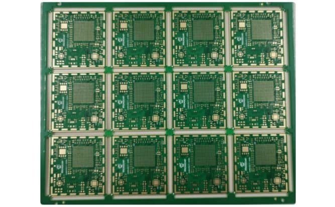
Panelized PCB sample from the PCBSync media library
PCBSync media-library sample illustrating panel format. Project-specific layer count and materials belong in the controlled fabrication record.

What should accompany the quotation?

  • Eighteen copper layers and seventeen intervals are accounted for.
  • Core copper is not counted twice.
  • Depth and diameter conventions are written down.
  • Mechanical and impedance reviews use the same stack revision.

Match the quoted construction, inspection scope and delivery requirements to the released revision. Confirm what is included before placing an order.

Specific questions

18 Layer PCB questions, answered.

What is the standard thickness of an 18 layer PCB?

There is no thickness defined solely by eighteen copper layers. Copper weights, dielectric gaps, material constructions and mechanical constraints determine the proposed build. Request a stack with tolerances instead of choosing from a universal thickness claim.

Should aspect ratio use drill diameter or finished-hole diameter?

Supplier conventions can differ. State the depth and diameter basis used, and ask the fabricator to confirm its capability convention. Keep both dimensions in the review when they are available.

Does a low geometric aspect ratio guarantee reliable plating?

No. It is a useful screening input, but material, drilling quality, cleaning, copper deposition and acceptance requirements also matter. The fabrication process and inspection plan must support the required construction.

Can I calculate the final thickness from prepreg datasheets?

You can prepare an initial budget, but unpressed material values do not establish the final dielectric gaps. Ask the fabricator for process-specific pressed values that account for the actual build and copper pattern.

When should the thickness budget be revisited?

Revisit it after changing layer count, copper weight, dielectric material, glass construction, hole spans or mechanical limits. Recheck controlled-impedance geometry and connector fit alongside the revised budget.

Engineering quotation

Request a 18-layer PCB review.

Start with the requirements you know. Include unresolved decisions so engineering can review the construction with you.

  • Eighteen copper layers and seventeen intervals are accounted for.
  • Core copper is not counted twice.
  • Depth and diameter conventions are written down.
  • Mechanical and impedance reviews use the same stack revision.

Attach fabrication data, the proposed stackup and quantity breaks when ready. For assembly, include the BOM, placement data and inspection requirements.

Discuss NDA arrangements before sharing confidential files. Ask for current certification scope and records relevant to your project.

Contact PCBSync · Include PCB assembly

One place for your enquiry

Continue on Contact

  1. Download the planning worksheet and review the open items.
  2. Send your requirements and available fabrication files on Contact.
  3. Agree the construction, inspection scope and quotation before ordering.
Request a project review →

Need an NDA or a particular file-transfer method? Contact us before sharing confidential files.

PCBSync engineering resources · Updated 1 October 2026 · Planning guidance and illustrations are not approved manufacturing stackups.