Inquire: Call 0086-755-23203480, or reach out via the form below/your sales contact to discuss our design, manufacturing, and assembly capabilities.
Quote: Email your PCB files to [email protected] (Preferred for large files) or submit online. We will contact you promptly. Please ensure your email is correct.
Notes: For PCB fabrication, we require PCB design file in Gerber RS-274X format (most preferred), *.PCB/DDB (Protel, inform your program version) format or *.BRD (Eagle) format. For PCB assembly, we require PCB design file in above mentioned format, drilling file and BOM. Click to download BOM template To avoid file missing, please include all files into one folder and compress it into .zip or .rar format.
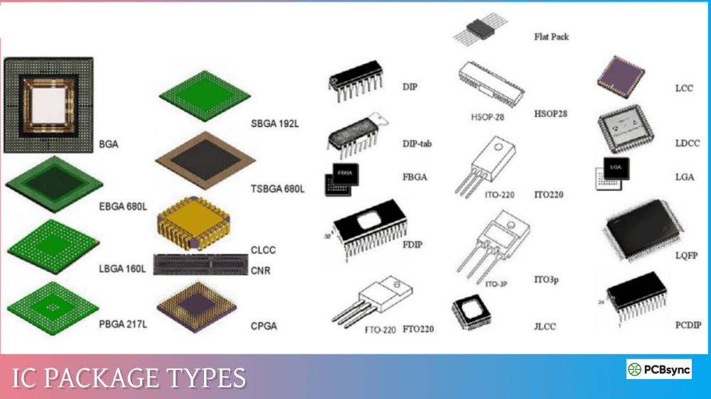
A ball grid array places its board connections underneath the component. That allows dense interconnection, but it also hides the joints that need inspection and repair. Choosing a BGA therefore commits the project to a footprint, an escape-routing strategy, an assembly process and an inspection plan. This guide focuses on those linked decisions. It explains package terminology without turning pin count into a guaranteed layer count or an X-ray image into proof that every electrical connection is sound.
1. Identify the exact package before designing the footprint
Start with the actual ball map. Original illustrative schematic; not a manufacturing limit or test result. Select the diagram to view full size.
BGA describes an external connection arrangement, not a complete internal construction. A package can connect its die to a substrate through different technologies, while the substrate presents an array of solder balls to the PCB. Terms such as plastic BGA and flip-chip BGA describe different aspects of construction. They should not be treated as a simple performance ranking in which one label guarantees better thermal or electrical behavior.
Start with the exact orderable device and package drawing. Record the package code, body outline, ball pitch, populated and unpopulated positions, orientation convention and recommended land pattern. Two devices with a similar body size may have different maps or missing-ball locations. A library footprint that looks plausible in three dimensions can still connect the wrong functions if the ball map is mirrored or the package variant is incorrect.
Check which view the manufacturer uses for the ball map. A top-view drawing and a bottom-view drawing cannot be copied into the same coordinate interpretation without review. Verify the first-ball marker against the schematic pin mapping, PCB footprint and assembly drawing. Have the reviewer trace several identifiable power, ground and signal locations through all three documents rather than relying only on the package outline.
Texas Instruments provides a BGA package search with device-package information. Use the applicable manufacturer’s drawing for the actual part. A family-level guide is useful context, but package-specific instructions take priority when they differ from a generic recommendation. Record the document revision used to create the library item.
Package-on-package adds another assembly interface above the board-mounted package. Its height, alignment, materials and thermal history must be reviewed as a system. It does not remove the need to inspect or validate the lower joints. Before selecting the arrangement, confirm that the intended assembly and test partners can review the exact configuration and provide the required evidence. Do not infer that capability from the availability of a placement machine alone.
Package terms describe construction, not a guaranteed result
A BGA uses an underside array of solder balls for electrical and mechanical connection to the PCB. PBGA refers to a plastic package construction; CBGA uses a ceramic construction; TBGA uses a tape substrate. Flip-chip describes how the die connects internally and can coexist with other package descriptors. Fine pitch describes spacing. Package-on-package describes a stacked arrangement. None of these labels alone establishes thermal resistance, allowable board strain, layer count or reliability for a particular assembly.
High connection density can reduce the board area needed for a device, while the hidden joints create inspection and repair constraints. Compare the exact device specifications and thermal path with the intended enclosure, board construction and operating conditions. A package without exposed leads can still suffer warpage, moisture damage or joint fatigue; handling and qualification remain necessary.
2. Plan escape routing using the real ball map
Can a trace fit between pads. Original illustrative schematic; not a manufacturing limit or test result. Select the diagram to view full size.
Pin count alone cannot determine the required PCB layer count. Routing demand depends on which balls are used, their positions, pitch, pad geometry, trace and spacing rules, via technology and reference-plane requirements. A table that assigns one layer count to every package with a particular number of balls hides these dependencies. Treat such tables as rough context, never as a released stack-up.
Classify the ball map before routing. Mark power and ground connections, high-speed interfaces, timing-sensitive groups, analogue signals and unused positions. Identify which nets must remain together or preserve a particular reference structure. Then test an escape concept using the proposed fabrication rules. The result should show actual paths through the constrained regions, not merely a count of available signal layers.
For an illustrative geometric screen, suppose adjacent copper pads have a center pitch of 0.80 mm and a diameter of 0.40 mm. The nominal gap between copper edges is 0.40 mm. One 0.10 mm trace with 0.10 mm clearance on both sides occupies 0.30 mm, leaving 0.10 mm nominal margin. Two such traces with three 0.10 mm spaces require 0.50 mm and do not fit that simple corridor. These are invented dimensions for explaining the calculation, not a PCBSync capability or a recommended footprint.
The screen does not account for via lands, neck-down rules, etch tolerances, routing direction or mask requirements. It also says nothing about whether the chosen width meets impedance needs. Use it to reject an obviously impossible idea early, then verify the actual layout with the agreed rules and stack-up. Record any reliance on finer features so it is visible during quotation.
Review vias and reference changes together. A routing solution that reaches every ball can still create an unsuitable return path or an unmanufacturable via structure. If via-in-pad is proposed, specify the required construction and surface condition instead of assuming that an ordinary open via beneath a solder ball is acceptable. Resolve the construction with fabrication and assembly before finalizing the footprint.
3. Connect land geometry, paste deposition and heating
Three geometries, one assembly. Original illustrative schematic; not a manufacturing limit or test result. Select the diagram to view full size.
The copper pad, solder mask opening and stencil aperture describe three different features. Changing one does not automatically correct the others. A copper pad may be defined primarily by its copper edge or by the solder mask opening, depending on the intended package land pattern. Follow the device guidance and the agreed manufacturing process; avoid a universal instruction to use one pad style for every BGA.
Review the paste print as a controlled deposition process. The stencil design, paste product, printing conditions and measured deposit all affect what reaches the joint. A ball already attached to the component does not make paste-volume review unnecessary. Equally, a generic instruction to add more paste can introduce other problems. Record the intended aperture approach and how initial deposits will be checked.
Develop the thermal profile around the actual assembly. Large components, copper distribution and board support can create different temperature histories at different locations. The oven program is an input; measured board and component temperatures are evidence. Use the thermal profiling workflow to connect sensor locations, material guidance and acceptance limits.
Include component handling and moisture-sensitive-device requirements from the actual packaging documentation. Track exposure and storage under the applicable procedure. Do not copy a generic baking temperature into a work instruction for every device, because component construction, packaging and permitted treatments differ. A material-handling issue should not be hidden by increasing the reflow temperature.
For the first article, keep the footprint revision, stencil revision, paste identity, placement program and measured profile together. If a defect is found, this record allows the team to investigate the same configuration. Without it, an apparently successful second trial may be impossible to reproduce. The useful deliverable is a repeatable process with defined evidence, not a claim that self-alignment during reflow will correct arbitrary placement or footprint errors.
4. Match inspection methods to the defect question
Inspection methods answer different questions. Original illustrative schematic; not a manufacturing limit or test result. Select the diagram to view full size.
BGA inspection begins by asking what must be detected. Optical inspection can examine package position and accessible features, but it cannot directly see every hidden joint. X-ray can reveal useful information about solder distribution and certain geometric defects. Electrical testing evaluates connections or functions within its coverage. None of these methods should be described as a universal substitute for the others.
A two-dimensional projection combines features along the X-ray path. Apparent overlap, void-like regions or unusual ball shapes need interpretation in the context of the package and board. Tilted views or three-dimensional methods may help resolve particular questions, but the appropriate method depends on the equipment, joint geometry and suspected failure mechanism. Specify the inspection objective rather than requesting “100% X-ray” without defining what will be assessed.
TI’s flip-chip BGA reference guide discusses inspection methods and their limitations for that package context. Use package guidance alongside the contractually applicable acceptance criteria. Do not copy one void percentage or illustrative image into a universal pass/fail rule for all BGA joints, especially when the feature type or measurement method differs.
Create an inspection matrix with four columns: suspected defect, available method, known limitation and escalation action. A bridge suspicion may require imaging and electrical correlation. An intermittent open may require a different investigation from a plainly missing ball. A functional pass demonstrates only the tested functions under the tested conditions; it does not prove every unused or redundant connection is sound.
Preserve evidence before destructive analysis or rework. Record the location, test result, image settings where relevant and board identity. If a joint is repaired immediately, the original failure evidence may disappear. Decide whether the investigation requires additional imaging, a controlled electrical test or specialist failure analysis before heating the component again. This sequence makes the result more useful than a collection of unlabelled X-ray screenshots.
5. Release the BGA with a documented review and rework boundary
BGA release: close the interfaces. Original illustrative schematic; not a manufacturing limit or test result. Select the diagram to view full size.
A practical release review follows one component from library selection to final test. Confirm the orderable part and package code, ball-map orientation, footprint revision, escape-routing rules, via construction, paste-print plan, thermal guidance and inspection coverage. Each item should point to a document or record. “Reviewed” without a revision or evidence reference gives the next engineer little to reproduce.
Use a small exception log for unresolved issues. For example, a proposed via construction might still need fabrication approval, while the package orientation is already confirmed. Keep those statuses separate. A completed schematic review does not close a fabrication exception. Name the decision owner and the evidence needed for closure, then release only under the agreed project process.
For loose-device work, define the IC reballing scope and acceptance requirements separately from board removal, installation and retest. Define the rework boundary before the first production run. Identify who can authorize removal, what thermal and handling guidance applies, how the site will be prepared and what inspection or retest follows. Do not assume that every assembly can tolerate an unlimited number of heating cycles. Underfill, adjacent components, board condition and package restrictions can change whether repair is practical.
When comparing suppliers, ask about the proposed evidence for your package rather than collecting broad equipment claims. A meaningful response explains how the actual footprint, stack-up and inspection requirement will be reviewed, which assumptions remain open and what additional work is quoted separately. This is more useful than a blanket promise of zero defects.
The deliverable should include an agreed manufacturing data set, a controlled assembly route and an inspection plan that states both coverage and limitations. Retain useful package-family information as background, but keep project decisions tied to the exact device. For detailed process discussion, continue to the BGA assembly page. This package guide supports selection and release planning; it does not certify a device, predict yield or replace the manufacturer’s documentation.
Related design and manufacturing resources
Bring the escape-routing plan and proposed multilayer PCB stackup to fabrication review, then include the package drawing and placement data in the BGA assembly request. Confirm the agreed via treatment and inspection scope before releasing the build.
For device-family context, see the integrated circuits guide. Read the applicable package drawing and documentation from the Texas Instruments website, Intel website or the selected device manufacturer. Contract requirements may refer to publications from IPC and JEDEC; confirm the required document and revision rather than treating a generic web guide as an acceptance standard.