Contact Sales & After-Sales Service

Contact & Quotation

  • Inquire: Call 0086-755-23203480, or reach out via the form below/your sales contact to discuss our design, manufacturing, and assembly capabilities.
  • Quote: Email your PCB files to [email protected] (Preferred for large files) or submit online. We will contact you promptly. Please ensure your email is correct.
One place for your enquiry

Continue on Contact

  1. Download the planning worksheet and review the open items.
  2. Send your requirements and available fabrication files on Contact.
  3. Agree the construction, inspection scope and quotation before ordering.
Request a project review →

Need an NDA or a particular file-transfer method? Contact us before sharing confidential files.

Notes:
For PCB fabrication, we require PCB design file in Gerber RS-274X format (most preferred), *.PCB/DDB (Protel, inform your program version) format or *.BRD (Eagle) format. For PCB assembly, we require PCB design file in above mentioned format, drilling file and BOM. Click to download BOM template To avoid file missing, please include all files into one folder and compress it into .zip or .rar format.

PCB manufacturing / dense routing, plane references and coupling

8 Layer PCB.
More routing freedom. Deliberate references.

Plan dense routing, signal references and power distribution together. Explore eight-layer allocations, compare thickness targets and prepare a focused fabrication RFQ.

Prototype & production requirements · Bare-board fabrication · Assembly available

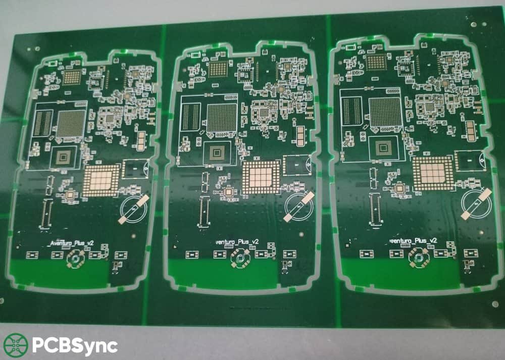
Panelized green PCB product sample with three routed board outlines
From the board, to your design.Panelized PCB product sample from the PCBSync media library. Review tooling, board separation and assembly requirements together.
Configure first

8 Layer PCB tools. One project brief.

Start with size, quantity and thickness. Compare the electrical layer assignment, record unresolved requirements, then prepare a project brief for Contact.

Engineering worksheet · no sign-up

Signal-to-reference matrix

Identify a reference for each critical routing layer and review adjacent signal-layer coupling.

Enable JavaScript to use this worksheet. You can also send your requirements through Contact.

Discuss this project →

Inputs stay in this page until you download them. Nothing is submitted automatically. Review the worksheet, then attach it on Contact.

WORKED ENGINEERING EXAMPLE

Extra routing layers still need a return-path plan

Hypothetical design scenario · Original conceptual diagram · Not a customer case or approved fabrication specification

Extra routing layers still need a return-path plan. Original conceptual engineering diagram; hypothetical values.01Group A routing02Reference continuity03Group B coupling review
Group A routing · Reference continuity · Group B coupling review. Diagram is not to scale.

A hypothetical design assigns two busy signal groups to neighboring internal layers to relieve congestion. That increases routing resources but does not prove that coupling is acceptable. Use the eight-layer proposal to inspect actual plane placement, dielectric spacing and parallel-route overlap, not just the number of signal layers.

Use this in your design review

  1. Assign each signal group a routing layer and reference conductor.
  2. Identify neighboring signal layers and long parallel runs.
  3. Review return transitions and via discontinuities before accepting the extra routing resources.

What to bring to the review

Record the geometric assumptions and the analysis or measurement needed for critical interfaces. Compare the six-layer alternative on the same routing constraints.

Discuss this construction →
Board specifications, layer concepts & fabrication brief
PCBSync engineering workbench

8 Layer PCB design & cost planner

Plan the board. Compare the construction. Prepare a useful RFQ.

Enable JavaScript for the planner, or use the Contact page. No sign-in or design-file upload is needed to explore the tool.

01 / Your board specification

02 / Electrical structure

Compare the role of each copper layer before committing to a layout. Coloured rows show electrical assignments, not dielectric dimensions or a pressed stackup.

Confirm material grade, copper, dielectric spacing, impedance and tolerance with engineering. Extra layers alone do not guarantee a continuous return path.

Electrical concept

Signal / ground / power · not to scale

Engineering limits and data storage

This tool prepares specifications; it does not inspect files or issue a price, approved stackup, impedance result or delivery commitment. Non-personal specifications may be retained in this browser tab for two hours. Download and review your brief before sending it through Contact.

Understand the construction

What is an 8 layer PCB?

An 8 layer PCB has eight copper layers. Designers can allocate the extra layers among signals, ground and power to address routing density and reference requirements. The layer count does not itself guarantee signal integrity. Dielectric spacing, signal grouping, power integrity and via transitions remain part of the design.

This page focuses on 8 layer PCB. For material families, layer-count tradeoffs and manufacturing routes, return to the multilayer PCB overview. For wider construction choices, see our PCB manufacturing planner.

Structure before routing

Choose the electrical allocation. Then confirm the physical stack.

These are planning choices, not released material recipes. Layer roles, pressed dielectric thicknesses, copper and the finished-board tolerance must be reviewed together.

ChoiceWhat it changesReview before release
S / G / S / G / P / S / G / SFour signal layers with three ground layers and one power layer.Check L3 and L6 against adjacent planes and specify which interface uses each route. Review power-referenced structures explicitly.
S / G / P / S / S / P / G / SAlternative plane allocation with adjacent inner signal layers.Assess coupling between L4 and L5; their spacing and routing geometry need a deliberate SI review.
1.0 or 1.2 mm targetCompact construction with eight copper layers.Review available dielectric builds, copper and through-hole geometry before assuming the thin target is feasible.
1.6 mm targetOne mechanical target for an eight-layer design.Choose the electrical spacing first and balance the full stack. Nominal overall thickness does not define a standard recipe.
2.0 or 2.4 mm targetThicker construction for the product’s mechanical needs.Review drill aspect ratio and unused via stubs. Discuss backdrilling where justified by the actual signal and geometry.
A prepreg glass-style name is not a guaranteed pressed thickness. Use the selected material system, resin content, copper distribution and the manufacturer’s proposed construction. The thickness checker above adds user-entered geometry; it does not predict lamination.
Design for a buildable board

8 Layer PCB design tips that change the next decision.

01 / Signal groups

Allocate interfaces before individual traces

Map critical interfaces to suitable reference structures, and separate their routing constraints from lower-speed control nets. Preserve a continuous nearby reference. More routing layers are useful only when the transition and reference strategy remains clear.

02 / Coupling

Examine adjacent inner signal layers

If two signal layers face one another, assess their spacing, parallel overlap and aggressor / victim behaviour. Orthogonal routing may help some geometries, but it is not a universal crosstalk cure. The stackup and signal requirements determine whether that allocation is acceptable.

03 / Vias

Account for the unused barrel

For fast interfaces, a via stub may warrant analysis. Board thickness, via endpoints and the interface’s edge rate matter together. Provide a backdrill map and controlled depth requirements if the design needs that process; keep it separately identified in the quotation.

FOLLOW THE RETURN PATHContinuous referenceKeep the nearby reference continuous.Split referenceA split can force a longer return route.Concept only. Actual current distribution depends on frequency and the full structure.
Return-path concept, not an electromagnetic simulation.

Make impedance a complete requirement.

Specify the target, tolerance, signal layer, reference layer and trace structure. Add the material and fabrication notes that control the geometry. A nominal target such as 50 Ω is incomplete without its construction and acceptance plan.

Explore controlled-impedance manufacturing and the impedance calculator. Use early calculations to frame the review, then agree the stackup before final routing.

For hole geometry, the drill aspect-ratio checker is a useful planning aid. Confirm whether a value refers to a drilled hole or a finished plated hole.

Mechanical and electrical fit

Specify thickness without losing the stackup.

Start with the product’s constraints.

Connector engagement, enclosure clearances, board support and assembly handling can constrain the finished thickness. Record the target and acceptable tolerance in the fabrication drawing. Include copper and coating assumptions when comparing a calculated total with the nominal board thickness.

For 8 layer PCB, do not assume a thinner board is cheaper or that a thicker one is electrically safer. Dielectric availability, hole geometry, material choices and the process route can outweigh the nominal thickness.

Separate a target from an approved recipe.

The tool offers mechanical targets for discussion. Feasibility depends on the combined layer count, copper, materials and features. A thickness target alone does not establish a buildable material construction.

Ask for a stackup drawing that identifies material, copper, pressed dielectric spacing, finished thickness and tolerances. Keep the approved drawing with the released fabrication files so repeat orders use the same controlling requirements.

What controls the price

Compare 8 layer PCB costs on the same specification.

01 / Construction

Layers are one part of the cost

Board area, material, copper and finish enter the base comparison. Dense features, unusual tolerances and complex vias can change the manufacturing route. Keep required electrical and reliability constraints when discussing cost reductions.

02 / Batch

Compare quantity breaks

Tooling and setup are spread over the batch. Panel utilization and production quantity affect the commercial quote. Compare the same revision at prototype and intended production quantities, with consistent inspection requirements.

03 / Scope

Separate the unpriced additions

Impedance verification, special vias, material substitutions, expediting, assembly, freight and taxes must be identified. A planning estimate with those items excluded cannot be compared directly with a fully scoped production quote.

Construction & verification

Connect the construction to the inspection plan.

Review areaEvidence to agree
Fabrication releaseRevision-controlled Gerber and drill files, material / stackup approval and resolved engineering questions.
Bare-board electrical testContinuity and isolation test scope against the agreed netlist. This is different from a powered functional test of an assembly.
Critical structuresProject-relevant inspection or cross-section requirements for holes, copper and material construction.
Controlled impedanceSpecified structures, tolerances and coupon / measurement requirements where requested.
Repeat productionRevision and change control, agreed acceptance records and disposition of any approved substitution.

Explore PCB electrical testing, the PCB laboratory and quality control. Request applicable certification scope and evidence during supplier qualification.

Questions before release

8 Layer PCB questions, answered.

Should an 8 layer PCB always use four signal layers?

No. Four signal layers are one planning allocation. Power rails, critical interfaces and reference requirements may lead to a different assignment. Review adjacent signal coupling and the actual pressed construction before release.

Is 1.6 mm a required thickness for an 8 layer PCB?

No. Finished thickness is a design and manufacturing requirement, not a consequence of layer count. Confirm the target and tolerance against the enclosure, connectors, materials, copper and dielectric build.

Can I use the electrical diagram as a fabrication stackup?

No. It shows copper-layer roles only. A fabrication stackup also needs material grades, pressed dielectric thicknesses, copper, finished thickness and tolerances. Confirm that construction with engineering.

Does this worksheet issue a quotation?

No. The worksheet records requirements and open questions. Request a reviewed quotation on Contact; price and schedule depend on files, materials, process details, quantities and agreed inspection scope.

What should I send if the design is not finished?

Start with the layer count, approximate size, quantities, target thickness, interfaces, material needs and open questions. Share the proposed layer map if available. A complete final quotation may need released fabrication data.

Can manufacturing and assembly be reviewed together?

Yes. Include the BOM, placement data, assembly drawing and test requirements with the board specification. Confirm panelization, finish, component supply and inspection scope across both services.

Engineering quotation

Request your 8 Layer PCB quote.

Send the current revision and the requirements that decide the build. If the design is still evolving, start with a brief and identify what remains open.

  1. Fabrication data: Gerber, drill files, outline and revision.
  2. Construction: layer map, material, target thickness, copper and finish.
  3. Electrical requirements: impedance targets, reference layers, vias and test scope.
  4. Commercial scope: quantity breaks, required timing and assembly needs.

Use Prepare text for Contact to copy your worksheet into your message, or download and attach it. Nothing is sent or transferred automatically.

For a supplier review, ask for the current certification scope and project-relevant inspection records. Discuss NDA arrangements before sending confidential design files.

Prefer a direct conversation? Contact PCBSync.

One place for your enquiry

Continue on Contact

  1. Download the planning worksheet and review the open items.
  2. Send your requirements and available fabrication files on Contact.
  3. Agree the construction, inspection scope and quotation before ordering.
Request a project review →

Need an NDA or a particular file-transfer method? Contact us before sharing confidential files.

PCBSync engineering resources · Updated 30 September 2026 · Diagrams are planning concepts; project-specific manufacturing requirements need confirmation.